Add to Cart
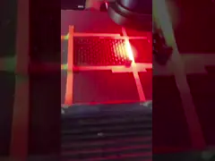
Soldering Pallets Processing Multiple Boards at The Same Time
we have advanced capabilities in machining and drilling composite materials. we can provide a wide range of manufacturing solutions for wave solder pallets that are custom-engineered and manufactured to each client's specifications.
The use of wave solder pallets, leads to overall process efficiency which can be improved by:
1. Reducing set-up time.
2. Wave solder complex, double-sided circuit board assemblies.
3. Eliminating expensive, and labour-intensive masking.
4. Shielding of heat-sensitive components.
5. Processing multiple boards at the same time.
6. Reducing bridging and skipping.
7. Increasing production and enhance automated assembly.
Wave solder pallets are made of composite materials with
advantageous features such as:
1. High temperature compatibility to endure repeated cycles through
the re-flow.
2. Dimensional stability to ensure board alignment is consistent.
3. Very low moisture absorption.
4. Low heat absorption.
5. Chemical resistance for increased durability through the harsh
cleaning process.
Specification:
| Model | DurostoneCHP760 | DurostoneCAS761 | DurostoneCAG762 |
| Grade | Standard | Anti-Static | Anti-static(Optical) |
| Colour | Blue | Black | Grey |
| Density(g/mm3) | 1.85 | 1.85 | 1.85 |
| Standard OperationTemperature | 260 | 260 | 260 |
| Maximum Operation Temperature(C) | 350 | 350 | 350 |
| Sheet Size(mm) | 2440×1220 | 2440×1220 | 2440×1220 |
| Tickness/weight(mm/kg) | 3/17, 4/22 | 5/28, 6/33, 8/44 | 10/55, 12/66 |
Working your way around the underside of the PCB, identify which
components
are parallel and perpendicular to the wave and assess the
solderability of each
PTH connector by comparing the actual separation against the graph
right.
Ideally you want to be above the line in all cases.
PCB Design Implications - for Board Designers - or respin
We are often called upon by our customers to help with identifying design respin opportunities.
We will identify problem areas within a board and suggest appropriate movements of components. (Ideally before the PCB is fabricated)
However for board designers reading this, can you remember another
four "rules" (to compete with the hundred other rules you have to
have floating
around in your head).
Keep large (height) SMT components away from PTH areas.
Leave the leading and trailing areas around PTH components as clear
as possible.
DON'T put any SMT components within 3mm (0.12") of any PTH
components.
DON'T put all PTH components in line along one edge of a board -
leave some space to allow us to support the masking in the centre
of the board.
Production flow