Add to Cart
Composite Solder SMT Trays Surface Mount Process Carriers
Durability
1. High-temperature compatibility to endure repeated cycles through
the re-flow.
2. Material stability to ensure board alignment is consistent.
3. Chemical resistance for increased durability through harsh
cleaning process.
Surface Mount Process Carriers have many features and benefits
which enhance automated assembly and increase production by:
1. Reducing set-up time.
2. Eliminating unnecessary PCB board handling by operators.
3. Minimizing board warping.
4. Eliminate expensive hand masking and labour costs.
5. Standardizing process repetition.
6. Machine parameters.
7. Minimizing soldering defects
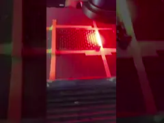
Surface Mount Process Carriers are engineered to completely fixture
a circuit board during the overall assembly process. These carriers
are made of high-temperature semi-conductive composite materials,
used from start to finish in the assembly process..
Specification:
| Model | DurostoneCHP760 | DurostoneCAS761 | DurostoneCAG762 |
| Grade | Standard | Anti-Static | Anti-static(Optical) |
| Colour | Blue | Black | Grey |
| Density(g/mm3) | 1.85 | 1.85 | 1.85 |
| Standard OperationTemperature | 260 | 260 | 260 |
| Maximum Operation Temperature(C) | 350 | 350 | 350 |
| Sheet Size(mm) | 2440×1220 | 2440×1220 | 2440×1220 |
| Tickness/weight(mm/kg) | 3/17, 4/22 | 5/28, 6/33, 8/44 | 10/55, 12/66 |
Our sales network
This estimation may be done in three ways
If a PCB is available (preferably populated) - our sales engineers
can rapidly evaluate your board.
If PCB design data is available we will process, analyse and
remotely assess it.
You can do it using the rules presented below - our customers
quickly find that the above two methods are easiest.
Gerber, Excellon and other data required
Pin Land to SMT pad clearance evaluation
The two figures below each show part of a CSWSC in plan and section
views. The right hand figure shows that more clearance
is required when the connector orientation is perpendicular to the
wave.
PTH Components Located Parallel to direction through wave
The clearance required between the pin land and SMT pad can be made
quite
small, as the solder does not have to flow "under" the component
pockets.
PCB Design Implications - for Board Designers - or respin
We are often called upon by our customers to help with identifying
design respin opportunities.
We will identify problem areas within a board and suggest
appropriate movements of components. (Ideally before the PCB is
fabricated)
However for board designers reading this, can you remember another
four "rules" (to compete with the hundred other rules you have to
have floating
around in your head).
Keep large (height) SMT components away from PTH areas.
Leave the leading and trailing areas around PTH components as clear
as possible.
DON'T put any SMT components within 3mm (0.12") of any PTH
components.
DON'T put all PTH components in line along one edge of a board -
leave some space to allow us to support the masking in the centre
of the board.