
Add to Cart
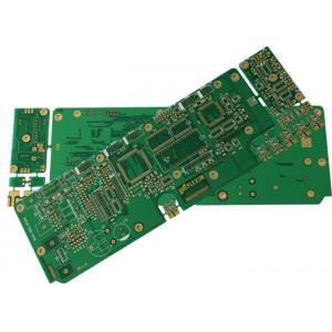
Multilayer Through Hole Blind Buried Vias 10 Layer PCB Circuit Board
Quick detail:
| Origin:China | Special: 10 layer |
| Layer:10 | Thickness:2.0mm |
| Surface: ENIG | Hole:0.8 |
Parameter:
| XCE PCB technical specifications | ||
| Annual stock Material | Rogers,Taconic,Arton,Isola,F4B,TP-2.FR-4,High TG,Halogen free | |
| Layer No. | 1~16 multilayer pcb | |
| Min board thickness | 2 layer0.2mm 4 layer0.4mm 6 layer 0.6mm 8 layer 0.8mm 10 layer 1.0mm | |
| Max panel size | 508*610mm | |
| Board thickness tolerance | T≥0.8mm±8%.,T<0.8mm±5% | |
| Wall hole copper thickness | >0.025mm(1mil) | |
| Finished hole | 0.2mm-6.3mm | |
| Min line width | 4mil/4mil(0.1/0.1mm) | |
| Min bonding pad space | 0.1mm(4mil) | |
| PTH aperture tolerance | ±0.075mm(3mil) | |
| NPTH aperture tolerance | ±0.05mm(2mil) | |
| Hole site deviation | ±0.05mm(2mil) | |
| Profile tolerance | ±0.10mm(4mil) | |
| Board bend&warp | ≤0.7% | |
| Insulation resistance | >1012Ωnormal | |
| Through-hole resistance | <300Ωnormal | |
| Electric strength | >1.3kv/mm | |
| Current breakdown | 10A | |
| Peel strength | 1.4N/mm | |
| Soldmask regidity | >6H | |
| Thermal stress | 288℃20Sec | |
| Testing voltage | 50-300V | |
| Min buried blind via | 0.2mm(8mil) | |
| Outer copper thickness | 1oz-5oz | |
| Inner cooper thickness | 1/2 oz-4oz | |
| Aspect ratio | 8:1 | |
| SMT min green oil width | 0.08mm | |
| Min green oil open window | 0.05mm | |
| Insulation layer thickless | 0.075mm-5mm | |
| Taphole aperture | 0.2mm-0.6mm | |
| Special technology | Indepedance,Blind buried via,thick gold,aluminum PCB | |
| Surface finish | HASL,Lead free HASL,Immersion Gold, Immersion Tin, Immersion Silver,OSP ,ENIG ,Golden finger,Blue glue,Gold plating | |
Files:Gerber,protel,powerpcb,Autocad,etc.
Material:FR-1,FR-4,CEM-1,CEM-3,HI-TG,Aluminum
Layer count:1-24 layers multilayer pcb
Max.Panel Size:450*1500mm
Board Thickness:0.2-5mm
Min. Core Thickness:0.075mm
Cu Thickness:12-140um
Min. Drill Size:0.2mm
Max. Aspect Ratio: 8:1
Min. Trace Width: 0.1mm
Min line spacing:0.075mm
Min. SMT/QFP Pitch:0.4mm
v Fast PCB Fabrication for Samples and Mass Production
v Electronic Components Sourcing Services
v PCBA Assembly Services:SMT,DIP,BGA...
v Function Test
v Stencil,Cable and Enclosure Assembly
v Reverse engineering service
v Standard Packing and On time Delivery
Typical Applications
Radio frequency (RF) and microwave PCB’s are a type of PCB designed to operate on signals in the megahertz to gigahertz frequency ranges (medium frequency to extremely high frequency). These frequency ranges are used for communication signals in everything from cellphones to military radars. The materials used to construct these PCB’s are advanced composites with very specific characteristics for dielectric constant (Er), loss tangent, and CTE (co-efficient of thermal expansion).
High frequency circuit materials with a low stable Er and loss tangent allow for high speed signals to travel through the PCB with less impedance than standard FR-4 PCB materials. These materials can be mixed in the same Stack-Up for optimal performance and economics.
Features
• High Thermal Performance
Tg: 180°C (DSC)
Td: 340°C (TGA @ 5% wt loss)
Low CTE for reliability
• T260: 60 minutes
• T288: 30 minutes
• RoHS Compliant
• UV Blocking and AOI Fluorescence
High throughput and accuracy during PCB
fabrication and assembly
• Superior Processing
Closest to conventional FR-4 processing
• Core Material Standard Availability
Thickness: 0.002″ (0.05 mm) to 0.125″
(3.2 mm)
Available in full size sheet or panel form
• Prepreg Standard Availability
Roll or panel form
Tooling of prepreg panels available
• Copper Foil Type Availability
Standard HTE Grade 3
RTF (Reverse Treat Foil)
• Copper Weights
½, 1 and 2 oz (18, 35 and 70 μm) available
Heavier copper available upon request
Thinner copper foil available upon request
• Glass Fabric Availability
Standard E-glass
Square weave glass fabric available
Spread glass fabric available
• Industry Approvals
IPC-4101C /21 /24 /26 /97 /98 /99 /101 /126
UL - File Number E41625 as PCL-FR-370HR
Qualified to UL's MCIL Program

