Primary / Dummy Grade Indium Phosphide Wafer Thickness 350um For LD
Brand Name:zmkj
Model Number:InP-2inch
Minimum Order Quantity:3pcs
Delivery Time:1-4weeks
Place of Origin:CHINA
Price:by case
Contact Now
Add to Cart
Verified Supplier
Location:
Shanghai Shanghai China
Address:
Room.1-1805,No.1079 Dianshanhu Road,Qingpu Area Shanghai city, China /201799
Supplier`s last login times:
within 13 hours
Product Details
Company Profile
Product Details
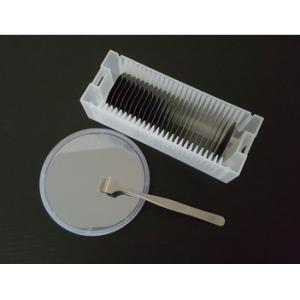
2inch N-type P-type thickness 350um primary grade Dummy grade Indium Phosphide crystal InP substrates wafer for LD
Indium phosphide single crystal material is one of most important semiconductor compound, which is key raw material for laser diode of indium phosphide substrate(LD), light emitting diode(LED), photodetector in optical communication production. Those parts play information launching, transmitting, amplifying, reception function .
Indium phosphide is ideal for high-frequency devices, as HEMT, HBT and so on.Because of its great property, it is widely used in fibre-optical communication, microwave, millietric wave, anti-radiation of solar cells, heterojunction transistor, other similar advanced technology and so on. Main production methods of indium phosphide single cryatal material include LEC, improved LEC, VCZ/PC-LEC, VGF, VB and so on.
Specification
| Item | Diameter | Type | carrying concentration | Mobility | Resistivity | MPD |
| S-InP | 2 | N | (0.8-6)X10^18 | (1.5-3.5)x10^3 | <500 | |
| 3 | <500 | |||||
| 4 | <1x10^3 | |||||
| Fe-InP | 2/3/4 | SI | >1000 | >0.5x10^7 | >5x10^3 | |
| Zn-InP | 2/3/4 | P | (0.6-6)X10^18 | 50-70 | <1x10^3 | |
| No dope InP | 2 | N | <3x10^16 | (3.5-4)x10^3 | <5x10^3 | |
| Other | ||||||
| Orientation | (100)/(111)±0.5° | Flatness | ||||
| TTV | Bow | Warp | ||||
| <12um | <12um | ≤15um | ||||
| 1st OF Flat | 16±2mm | 22±2mm | 32.5±2.5mm | |||
| 2st OF Flat | 8±1mm | 11±2mm | 32.5±2.5mm | |||
| Surface:1sp or 2sp ,2inch 350±25um,3inch 600±25um,4inch 625±25um,or by customized | ||||||
Most of our production is made up of premium grade wafers. However, in every boule, some test grade wafers are available. Test wafers have the same electrical
performance and geometrical specification than premium wafers but
with a small local damage :
- a surface defect like a scratch or a pit or a stain on the front side,
- a crystalline imperfection like high EPD or a twin lamellae. The latter is made up of 2 parallel lines in the <110> direction. Between these 2 lines, the orientation is not (100) contrary to the whole wafer ; the distance between the 2 lines is very small (< 1mm).
Over 95 % of the whole surface is premium quality which makes them useful for calibration runs. The type of defect is indicated on a label for each wafer.
sample
FAQ
Why choose us— ZMKJ .?
- 5 years experience in semi wafers & optics field;
- Professional workshop production line in our factory ;
- Specialized optics and wafers process knowledge;
- High quality control level;
- Small order acceptable;
- Customized Products as required;
- Experience for Cooperation for other country company.
Dealing Term
Delivery Time: 10-25 days
Shipping term: Exw factory, FOB Shanghai
Delivery term: Express service/Air freight
Payment term: T/T 100% in advance, or Deposit on order
Packaging & Shipping
As Optics mostly are small size, delivery we prefer to use Express.
It will be highly appreciate if you can provide Express account for delivery, thanks for supports!


Primary / Dummy Grade Indium Phosphide Wafer Thickness 350um For LD
Inquiry Cart
0