Test Grade Monocrystalline Silicon Wafer , High Resistivity Silicon Wafer
Brand Name:zmkj
Model Number:si-6inch
Minimum Order Quantity:25pcs
Delivery Time:5-30days
Place of Origin:china shanghai
Price:by case
Contact Now
Add to Cart
Verified Supplier
Location:
Shanghai Shanghai China
Address:
Room.1-1805,No.1079 Dianshanhu Road,Qingpu Area Shanghai city, China /201799
Supplier`s last login times:
within 13 hours
Product Details
Company Profile
Product Details
semiconductor wafer 6inch prime sillicon wafer, sillicon optical
lens, IC sillicon substrates , poly sillicon wafer,Semiconductor 3'
inch silicon wafer, single crystal ,2inch,
3inch,4inch,5inch,6inch,8inch,12inch silicon wafer, single side
polished silicon wafer
1. Description
| 2.4(g/cm3) | ||
| Dope type | no dope | doped B | doped P |
| Type | I | P | N |
| resistivity | Ø 1000Ωcm | 10-3~40Ωcm | 10-3~40Ωcm |
| E P D | ≤100∕cm2 | ≤100∕cm2 | ≤100∕cm2 |
| Oxygen content (∕cm3) | ≤1~1.8×10¹⁸ | ≤1~1.8×10¹⁸ | ≤1~1.8×10¹⁸ |
| Carbon content(∕cm3) | ≤5×10¹⁶ | ≤5×10¹⁶ | ≤5×10¹⁶ |
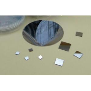
| Size | 10×3m,10×5m,10×10mm,15×15mm, | ||
| Dia50.8mm,Dia76.2mm,Dia100mm | dia6-12inch | ||
| or by customized size | |||
| thickness | 0.5mm,1.0mm or other | ||
| tolerance | <±0.1mm | ||
| thickness tolerance | <±0.015mm (or <±0.005mm) | ||
| surface | 1sp or 2sp | ||
| orientation | ±0.5° | ||
| orientation | <100>,<110>,<111> | ||
| package | 100grade in1000 grade cleaning room |
we receive customized size by any type!
2. specification for 4-6inch size.
| Name: 6Inch P-type 99.9999% Purity Price Silicon Wafer | ||
| Size | 4"/5"/6" | |
| Growth method | CZ | |
| Grade | Prime grade | |
| Diameter | 100±0.4mm / 125±0.5mm / 150±0.5mm | |
| Orientation | <111>/<100> | |
| Type | N-type/P-type | |
| Dopant | P-type:Boron | |
| N-type:Phos./As./Sb. | ||
| Purity | 11N(99.999999999%) | |
| Oxygen Content | ≤18 New PPMA | |
| Carborn Content | ≤1 New PPMA | |
| Resistivity | ≥0.001Ω·cm | |
| Thickness | ≥200um, or according to your requirement | |
| Others | TTV≤10um, Bow≤35um,Warp≤35um | |
| Particles | ≥0.3um@≤10PPW | |
| Surface | Frond side polished,back side etched. | |
| MOQ | 100pcs | |
| Package | Packed in cassette,and sealed in vacuum bag,25pcs/cassette. | |
| Price | According to your specification,especially resistivity and thickness | |
3 About our company
SHANGHAI FAMOUS TRADE CO.,LTD. locates in the city of Shanghai,
Which is the best city of China,
and our factory is founded in Wuxi city in 2014.
We specialize in processing a varity of materials into wafers,
substrates and custiomized optical glass parts.components widely
used in electronics, optics, optoelectronics and many other fields.
We also have been working closely with many domestic and oversea
universities, research institutions and companies, provide
customized products and services for their R&D projects.
It's our vision to maintaining a good relationship of cooperation
with our all customers by our good reputatiaon.
4. packing and delivery
-FAQ –
Q: Are you trading company or manufacturer ?
A: zmkj is a trading company but have a sapphire manufacturer and,
as a supplier of semiconductor materials wafers for a wide span of
applications.
Q: How long is your delivery time?
A: Generally it is 5-10 days if the goods are in stock. or it is
15-20 days if the goods are not in stock,
it is according to quantity.
Q: Do you provide samples ? is it free or extra ?
A: Yes, we could offer the sample for free charge but do not pay the cost of freight.
Q: What is your terms of payment ?
A: Payment<=1000USD, 100% in advance. Payment>=1000USD,
50% T/T in advance ,balance before shippment.
If you have another question, pls feel free to contact us as below:


Test Grade Monocrystalline Silicon Wafer , High Resistivity Silicon Wafer
Inquiry Cart
0