Add to Cart
High precision Electronic multilayer pcb assembly PCB manufacturer
Quotation needed
1).For PCB bare board, we'll quote in 1-2 hours based on PCB file and Gerber file;
2).For PCBA projects, our engineer quote in 12-24 hours(current day) based on BOM list;
3).For customized finished product, our detailed quotes will be valid in 1 week at most;
-Please advice?
(ALL information between customer & HUA XING are confidential, only for quotes and prodution.)
DIP Processing
SHINELINK has three DIP processing lines, professional working
platforms and carriers, this ensures a output capacity of 1 500
000pcs per day. For every process, technical and standard operation
guidelines are made to follow, with strict KPI, this makes sure of
99.8% of pass for every PCBA. Lower our rejects, create more value
for clients.
PCB Manufacturing Lead Time.
| Layer/Days | Sample(Normal) | Sample(Fast) | Mass Production |
| Single/Double | 2-3days | 24hours | 5-7days |
| Four Layer | 7-10days | 3days | 7-10days |
| Six Layer | 7-10days | 5days | 13-15days |
| Eight Layer | 15-20days | 7days | 15-20days |
PCB Assembly Capabilities
| Turnkey PCBA | PCB+components sourcing+assembly+package |
| Assembly details | SMT and Thru-hole, ISO lines |
| Lead Time | Prototype: 15 work days. Mass order: 20~25 work days |
| Testing on products | Flying Probe Test, X-ray Inspection, AOI Test, functional test |
| Quantity | Min quantity: 1pcs. Prototype, small order, mass order, all OK |
| Files we need | PCB: Gerber files(CAM, PCB, PCBDOC) |
| Components: Bill of Materials(BOM list) | |
| Assembly: Pick-N-Place file | |
| PCB panel Size | Min size: 0.25*0.25 inches(6*6mm) |
| Max size: 20*20 inches(500*500mm) | |
| PCB Solder Type | Water Soluble Solder Paste, RoHS lead free |
| Components details | Passive Down to 0201 size |
| BGA and VFBGA | |
| Leadless Chip Carriers/CSP | |
| Double-sided SMT Assembly | |
| Fine Pitch to 0.8mils | |
| BGA Repair and Reball | |
| Part Removal and Replacement | |
| Component package | Cut Tape,Tube,Reels,Loose Parts |
| PCB assembly process | Drilling-----Exposure-----Plating-----Etaching & Stripping-----Punching-----Electrical Testing-----SMT-----Wave Soldering-----Assembling-----ICT-----Function Testing-----Temperature & Humidity Testing |
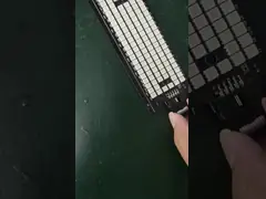
PCBA Picture