
Add to Cart
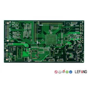
10 Layers Blind Vias Communication PCB Board Circuit with HASL Lead Free
Blind vias is designed in this PCB board. The aperture of blind via is 0.1 mm. And the Min. Line width / spacing are 0.08 / 0.05mm. This PCB is designed to used in communication device. And with certificated HASL lead free surface treatment make the product hamless to human body and more eco friendly.
Established in 1999, Lefang owns 3 modern Printed Circuit Board factories in Guangdong, China.
We provide One-stop solution for PCB & PCBA manufacturing to our customers home and abroad.
High quality PCB products, competitive price, on time delivery, after-sale service are always offered.
To make the continued progress, we try our best to in every section, including selecting quality raw materials
strictly, imported advanced automated equipments, employing 70 experienced engineers, acquiring global
certification of ISO9001:2008, ISO14001:2004, ISO/TS16949:2009, UL, QC080000, OHSA18000, etc.
Our customers' industry come from Communication, Industrial Control, Automotive, Medical Equipment,
Security Apparatus, Consumer Electronics and LED Lighting.
We sincerely pursue win-win business with customer all the time!
| Step 1 Please send us Gerber file with these format: .CAD / .Gerber / .PCB / .DXP / .P-CAD, etc | ||||||||||||||||||||
| Step 2 Also please provide us the below details for quick quotation: | ||||||||||||||||||||
Board material: Fr - 4 / CEM - 1 / CEM - 3 / 22F / Fr - 1 / others | ||||||||||||||||||||
| Material brand: SY / KB / Rogers (optional) | ||||||||||||||||||||
| Material Specification:High Tg / copper based / aluminum based or others (optional) | ||||||||||||||||||||
| Board thickness: 0.1 - 6.0 mm | ||||||||||||||||||||
| Copper thickness: 0.05 Oz - 8 Oz ( 17 um - 288 um ) | ||||||||||||||||||||
| Surface Treatment: OSP / ENIG / HASL / Lead Free HASL / Immersion Tin / Immersion Sin | ||||||||||||||||||||
| Color of solder mask and silk print: Green / red / blue / black / white / yellow ,etc | ||||||||||||||||||||
| Board size and quantity | ||||||||||||||||||||
If you don't have Gerber file, please provide us the imfomation as step 2 or post your PCB Board to us for clone. | ||||||||||||||||||||
SAMPLE: | ||||||||||||||||||||
| ||||||||||||||||||||
Lead Time
| Layer count | Sample lead time/workday | Batch lead time/workday |
| 1-2L | 2 | 6 |
| 4L | 5 | 8 |
| 6L | 5 | 9 |
| 8L | 6 | 10 |
| 10L | 8 | 10 |
| 12L | 8 | 12 |
| 14L | 10 | 15 |
| 16L | 10 | 18 |
| 18-40L (Up to difficulty) | at least 18 | at least 24 |
| P.S. For HDI, Blind/Buried Hole PCB: Regular Lead Time + 3 workdays | ||
What kinds of test function will be offered?
| AOI (Automated Optical Inspection) | Impedance control |
| Automatic short-circuit testing | Metallographic microscope |
| RoHS detector | Fly probe/ fixture mold |
| Dielectric tester | Visual inspection |
Now send us your inquiry, and you will be replied within 8 hours!
Little knowledge - Single Sided PCB
Single sided PCB contains only one layer of conductive material, where components are focused on one side, and the other side of the wire is concentrated.
Single sided PCB are the best choice for low density designs. They are easily designed and quickly manufactured to serve as the most cost effective platform in the industry.
For surface finishes, single sided boards are available for Organic surface protectant (OSP), Immersion Silver, Tin, and Gold plating along with both leaded or lead-free Hot Air Solder Level (HASL), with operating temperatures range from 130℃ to 230℃.

