
Add to Cart
White Silkscreen 94V0 Fr4 PCB Board for Security Camera Display Devices
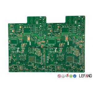
The double sided FR4 PCB Board is applied to security camera displayer, with 1.6 mm board thickness. The specification of the FR4 PCB Board is 210.5*143 mm, with green solder mask and OSP surface treatment. Its minimum aperture is 0.25 mm.
How to get quick quotation?
| Step 1 Please send us Gerber file with these format: .CAD / .Gerber / .PCB / .DXP / .P-CAD, etc | ||||||||||||||||||||
| Step 2 Also please provide us the below details for quick quotation: | ||||||||||||||||||||
Board material: Fr - 4 / CEM - 1 / CEM - 3 / 22F / Fr - 1 / others | ||||||||||||||||||||
| Material brand: SY / KB / Rogers (optional) | ||||||||||||||||||||
| Material Specification:High Tg / copper based / aluminum based or others (optional) | ||||||||||||||||||||
| Board thickness: 0.1 - 6.0 mm | ||||||||||||||||||||
| Copper thickness: 0.05 Oz - 8 Oz ( 17 um - 288 um ) | ||||||||||||||||||||
| Surface Treatment: OSP / ENIG / HASL / Lead Free HASL / Immersion Tin / Immersion Sin | ||||||||||||||||||||
| Color of solder mask and silk print: Green / red / blue / black / white / yellow ,etc | ||||||||||||||||||||
| Board size and quantity | ||||||||||||||||||||
If you don't have Gerber file, please provide us the imfomation as step 2 or post your PCB Board to us for clone. | ||||||||||||||||||||
SAMPLE: | ||||||||||||||||||||
| ||||||||||||||||||||
| Layer count | Sample lead time/workday | Batch lead time/workday |
| 1-2L | 2 | 6 |
| 4L | 5 | 8 |
| 6L | 5 | 9 |
| 8L | 6 | 10 |
| 10L | 8 | 10 |
| 12L | 8 | 12 |
| 14L | 10 | 15 |
| 16L | 10 | 18 |
| 18-40L (Up to difficulty) | at least 18 | at least 24 |
| P.S. For HDI, Blind/Buried Hole PCB: Regular Lead Time + 3 workdays | ||
What kinds of quality Raw Materials will be used?
| Board Brand | ITEQ, SY, Isola. Rogers, Arlon, Nelco, Taconic, Hitachi, KB,etc |
| Potion | Rohm & Haas, Atotech, Umicore |
| Printing Ink | Taiyo, Rongda |
| Dry Film | Asahi, Dupont, Etertec |
Now send us your inquiry, and you will be replied within 8 hours!
Little knowledge - How to improve the use ratio of PCB Board
1. Enlarge the PCB panel size, the larger panel, the less margin wasted;
2. Increase the pieces of PCB Board in each Sheet, which could also decrease the margin waste;
3. If two types of PCB such as A(big) and B(small), they could not reach a good use ratio when arrayed separately, then you could consider whether is suitable to array A and B in one sheet;
4. It is great to use professional software to arrange the PCB Board array.

