
Add to Cart
94V0 Circuit Board PCB for Automotive GPS System
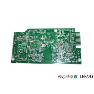
The 2 layers single sided copper base PCB is applied for Automotive GPS System, which board thickness is 1.6 mm. And its the minimum aperture is 0.2 mm and the line width and space are both 0.1 mm. While the surface treatment of the copper base PCB is LF-HSAL with green solder.
Established in 1999, Lefang owns 3 modern Printed Circuit Board
factories in Guangdong, China.
We provide One-stop solution for PCB & PCBA manufacturing to
our customers home and abroad.
High quality PCB products, competitive price, on time delivery, after-sale service
are always offered.
To make the continued progress, we try our best to in every
section, including selecting quality raw materials
strictly, imported advanced automated equipments, employing 70
experienced engineers, acquiring global
certification of ISO9001:2008, ISO14001:2004, ISO/TS16949:2009, UL,
QC080000, OHSA18000, etc.
Our customers' industry come from Communication, Industrial
Control, Automotive, Medical Equipment,
Security Apparatus, Consumer Electronics and LED Lighting.
We sincerely pursue win-win business with customer all the time!
How to get quick quotation?
| Step 1 Please send us Gerber file with these format: .CAD / .Gerber / .PCB / .DXP / .P-CAD, etc | ||||||||||||||||||||
| Step 2 Also please provide us the below details for quick quotation: | ||||||||||||||||||||
Board material: Fr - 4 / CEM - 1 / CEM - 3 / 22F / Fr - 1 / others | ||||||||||||||||||||
| Material brand: SY / KB / Rogers (optional) | ||||||||||||||||||||
| Material Specification:High Tg / copper based / aluminum based or others (optional) | ||||||||||||||||||||
| Board thickness: 0.1 - 6.0 mm | ||||||||||||||||||||
| Copper thickness: 0.05 Oz - 8 Oz ( 17 um - 288 um ) | ||||||||||||||||||||
| Surface Treatment: OSP / ENIG / HASL / Lead Free HASL / Immersion Tin / Immersion Sin | ||||||||||||||||||||
| Color of solder mask and silk print: Green / red / blue / black / white / yellow ,etc | ||||||||||||||||||||
| Board size and quantity | ||||||||||||||||||||
| ||||||||||||||||||||
SAMPLE: | ||||||||||||||||||||
| ||||||||||||||||||||
|
Now send us your inquiry, and you will be replied within 8 hours!
Comparison of PCB Surface Finish
As we all know, copper is easily oxidized when exposed in the air,
which is not good for welding with the electronics components.
Therefore, we need to protect the PCB copper by cladding a special
film. And we will compare 4 different surface finish as below to
make you understand more clearly:
Surface Finish Advantage Disadvantage
OSP Good welding Performance; Smooth Surface; RoHS; Cheap
Short-time Storage
HASL(Hot Air Solder Leveling) Good welding Performance; Long-time
storage; Cheap Unsmooth Surface; not RoHS compliance
Lead Free HASL Long-time storage; RoHS Unsmooth Surface; a little
expensive
ENIG(Immersion Gold) Good welding Performance; Smooth Surface; RoHS
Expensive

