Add to Cart
Sensor LED Double Sided OEM Prototype PCB Assembly pcb board, PCB factory,SMT Assembly,3 Mil
1. Features
1. One Stop OEM Service, Made in Shenzhen of China
2. Manufactured by Gerber File and BOM List from Customer
3. FR4 Material, Meet 94V0 standard
4. SMT, DIP technology suport
5. Lead Free HASL, Environmental Protection
6. UL, CE, ROHS Compliant
7. Shipping By DHL,UPS, TNT, EMS or Customer requirement
2. PCBA Technical capability
| SMT | Position accuracy:20 um |
| Components size:0.4×0.2mm(01005) —130×79mm,Flip-CHIP,QFP,BGA,POP | |
| Max. component height::25mm | |
| Max. PCB size:680×500mm | |
| Min. PCB size:no limited | |
| PCB thickness:0.3 to 6mm | |
| PCB weight:3KG | |
| Wave-Solder | Max. PCB width:450mm |
| Min. PCB width: no limited | |
| Component height:Top 120mm/Bot 15mm | |
| Sweat-Solder | Metal type :part, whole, inlay, sidestep |
| Metal material:Copper , Aluminum | |
| Surface Finish:plating Au, plating sliver , plating Sn | |
| Air bladder rate:less than20% | |
| Press-fit | Press range:0-50KN |
| Max. PCB size:800X600mm | |
| Testing | ICT,Probe flying,burn-in,function test,temperature cycling |
Certifications:
ISO9001 / ISO14001 / ISO45001 (Military) / TS16949 (Automotive) / RoHS / UL
Prototyping PCB assembly is the process of building and testing small-scale versions of printed circuit boards before proceeding to full-scale manufacturing. This stage is critical in the product development life cycle as it verifies the PCB’s design, functionality, and manufacturability.
The following are the key steps involved in prototype PCB assembly:
Design review:
Thoroughly review PCB design documents, including schematics and
layouts, to ensure designs meet functional and technical
requirements.
This review may involve checking for design rule violations,
component placement, signal routing, and overall manufacturability.
Component Selection and Procurement:
Select required electronic components such as integrated circuits,
resistors, capacitors, and connectors based on design
specifications.
These components are then sourced from reliable suppliers, ensuring
their availability and compliance with design requirements.
Prototype PCB Manufacturing:
PCB design files are sent to the PCB manufacturing facility, which
produces physical PCB prototypes.
This may involve processes such as copper plating, drilling and
solder mask application to create the required multi-layer PCB
structure.
Component assembly:
Electronic components are placed and soldered onto the prototype
PCB manually or semi-automatically.
This can be done using techniques like through-hole soldering,
surface mount soldering, or even advanced processes like reflow
soldering.
Inspection and Testing:
Thoroughly inspect the assembled prototype PCB for any
manufacturing defects, such as solder bridges, missing components,
or improper component orientation.
Functional testing is performed to verify the operation of the PCB,
including connectivity, signal integrity, and functionality of
individual circuits and subsystems.
Design iterations and refinements:
Based on the results of inspection and testing, the PCB design can
be refined or modified to solve any problems or optimize its
performance.
This iteration process continues until the prototype PCB meets the
required specifications and requirements.
Prototype PCB assembly is typically performed in small batches or single units, using
specialized equipment such as pick and place machines, reflow
ovens, and test equipment.
Prior to mass production, successful completion of the prototype PCB assembly phase is critical to ensure the reliability, functionality, and manufacturability of the final PCB product.
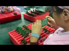
2. PCBA Pictures