Add to Cart
Printed Circuit Board Assembly Lead Free Surface Mount pcba board white Silk Screen
Features
Detailed Specification
| Material | FR4 |
| Finish Board Thickness | 1.6MM |
| Finsh Copper Thickness | 1OZ |
| Layer | 4L |
| Solder Mask Color | Green |
| Silkscreen | White |
| Surface Treatment | Lead Free |
| Finished Size | Customized |
What KAZ Circuit can do for you:
To get a full quotation of the PCB/PCBA, pls provide the
information as below:
Company Informaiton:
KAZ Circuit is a professional PCB manufacturer from China since
2007, also provide PCB Assembly service for our customers. Now with
about 300 employees. Certified with ISO9001,TS16949, UL, RoHS. We
are confident to provide you quality products with factory-directed
price within the fastest delivery time!
Manufacturer Capacity:
| Capacity | Double Sided: 12000 sq.m / month Multilayers: 8000sq.m / month |
| Min Line Width/Gap | 4/4 mil (1mil=0.0254mm) |
| Board Thickness | 0.3~4.0mm |
| Layers | 1~20 layers |
| Material | FR-4, Aluminum, PI |
| Copper Thickness | 0.5~4oz |
| Material Tg | Tg140~Tg170 |
| Max PCB Size | 600*1200mm |
| Min Hole Size | 0.2mm (+/- 0.025) |
| Surface Treatment | HASL, ENIG, OSP |
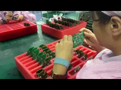
Customized PCB assembly process
PCB Design and Fabrication:
Collaborate with PCB design engineers to create schematics and layouts for custom PCBs.
Complete PCB design, including component placement, trace routing, and any special requirements.
Send design files to PCB manufacturer for fabrication.
Receive the bare PCB from the manufacturer and check for any defects.
Component purchasing:
Determine the required electronic components such as ICs, resistors, capacitors, and connectors.
Purchase necessary components from an authorized distributor or direct from the manufacturer.
Ensure components are compatible with the PCB design and meet the specifications of the project.
PCB Assembly:
Prepare the PCB for assembly by cleaning the surface and applying solder paste to component pads.
Use automated pick and place machines to place components accurately on the PCB.
Reflowing the solder paste in a controlled environment, such as a reflow oven, creates component connections.
Perform visual and electrical inspection of assembled PCBs to ensure proper component placement and solder joints.
Dedicated assembly process (if necessary):
Depending on the PCB design and application, additional assembly processes may be required, such as:
Through-hole component insertion and soldering
Ball Grid Array (BGA) or Chip Scale Package (CSP) component connections
Conformal coating or potting for environmental protection
Heat sink or thermal management component installation
Testing and Quality Assurance:
Perform various tests to verify functionality and reliability of custom PCBs such as:
Electrical testing (e.g. continuity, resistance, voltage and current measurements)
Functional testing to ensure PCB meets design specifications
Environmental testing (e.g. temperature, humidity, vibration) (if necessary)
Document test results and any problems encountered during assembly.
Final assembly and packaging:
Integrate custom PCB into final product or system (if applicable).
Pack PCBs or complete assemblies for safe shipping and delivery to customers.
Provide any necessary documentation such as assembly instructions, schematics, and test reports.
Throughout the custom PCB assembly process, manufacturers should maintain strict quality control procedures, adhere to industry standards, and ensure traceability of all components and processes.
Pictures