Add to Cart
FR4 Printed Circuit Boards 1oz Copper 1.0mm 4 Layers PCB Assembly Electronic Printed Circuit Board
Detail Specifications:
To get a full quotation of the PCB/PCBA, pls provide the
information as below:
|
|
|
What KAZ Circuit can do for you:
Electronic printed circuit board (PCB) assembly process
PCB design and manufacturing:
Work with PCB designers to create schematics and layouts for electronic PCBs.
Consider factors such as component placement, trace routing, and
design rules during layout.
Send the design files to the PCB manufacturer for manufacturing,
specifying the required layers, materials, and finishes.
Receive the bare PCB from the manufacturer and inspect it for any
defects or issues.
Component Procurement and Preparation:
Determine the electronic components required for the PCB, such as
integrated circuits (ICs), resistors, capacitors, and connectors.
Purchase the necessary components from an authorized distributor or
directly from the manufacturer.
Prepare components for assembly, ensuring they are correctly
oriented and lead-free (if applicable).
Automated PCB assembly:
Apply the solder paste to the PCB using a stencil printing process
or an automated dispenser.
Electronic components are accurately placed on the PCB using pick
and place machines.
Reflow soldering is performed in a controlled lead-free environment
to form reliable solder joints.
For through-hole components, use automated insertion and soldering
equipment.
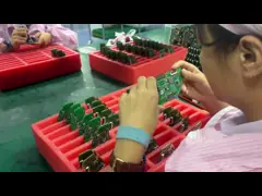
Inspection & Quality Control:
Visually inspect the assembled PCB to ensure correct component
placement and solder joint quality.
Perform electrical tests such as continuity checks, resistance
measurements, and power-on tests to ensure the PCB is functioning
properly.
Implement additional quality control measures, such as automated
optical inspection (AOI) or x-ray inspection, to detect any hidden
defects.
Optional selective soldering:
For specific components or areas of the PCB, use selective
soldering techniques such as hand soldering or selective wave
soldering.
This method is typically used for components or rework and repairs
that are difficult to solder using the reflow process.
Conformal coating and packaging:
A protective conformal coating is applied to the assembled PCB to
enhance its environmental and mechanical resilience.
In some cases, PCBs may be encapsulated in potting compound or
underfill material to provide additional protection and support.
Final checks and tests:
Extensive functional testing is performed to ensure that the
assembled PCB meets all design specifications and requirements.
Conduct environmental testing such as thermal cycling, humidity,
and vibration to verify PCB reliability and durability.
Document all test results and retain detailed quality records for
traceability.
Packaging and shipping:
Pack the PCB in an appropriate container or enclosure for safe
shipping and storage.
Provide any necessary documentation, such as assembly instructions,
schematics, and test reports, to accompany the PCB.
Key considerations for electronic PCB assembly:
Comply with industry standards and guidelines for PCB design and
manufacturing
Use high quality, reliable components and materials
Automation and process control to ensure consistent, repeatable
assembly
Rigorous inspection and testing throughout the entire assembly
process
Sturdy packaging and shipping methods to protect PCBs during
transit
The electronic PCB assembly process is designed to create reliable, high-quality PCBs
that meet the needs of a variety of electronic applications. A
combination of automated assembly techniques, quality control
measures and protective measures ensure PCB performance, durability
and long-term functionality.
More photoes of 2 layers FR4 1.0mm 1oz Immersion Gold printed circuit board PCB