Add to Cart
prototype development high-mix low-volume production SMT PCB Assembly
Detail Specifications:
| Layers | 2 |
| Material | FR-4 |
| Board Thickness | 1.6mm |
| Copper Thickness | 1oz |
| Surface Treatment | HASL LF |
| Soldmask & Silkscreen | Green & White |
| Quality Standard | IPC Class 2, 100% E-testing |
| Certificates | TS16949, ISO9001, UL, RoHS |
What KAZ Circuit can do for you:
To get a full quotation of the PCB/PCBA, pls provide the
information as below:
Manufacturer Capacity:
| Capacity | Double Sided: 12000 sq.m / month Multilayers: 8000sq.m / month |
| Min Line Width/Gap | 4/4 mil (1mil=0.0254mm) |
| Board Thickness | 0.3~4.0mm |
| Layers | 1~20 layers |
| Material | FR-4, Aluminum, PI |
| Copper Thickness | 0.5~4oz |
| Material Tg | Tg140~Tg170 |
| Max PCB Size | 600*1200mm |
| Min Hole Size | 0.2mm (+/- 0.025) |
| Surface Treatment | HASL, ENIG, OSP |
SMT Capacity
Prototype development high-mix low-volume production SMT PCB
Assembly
Definition:
Prototype development high-mix low-volume production SMT PCB
assembly refers to the process of assembling printed circuit boards
(PCBs) for prototype development and low-volume production runs
using surface mount technology (SMT). SMT is a method of assembling
electronic components directly onto the surface of a PCB, rather
than inserting them into holes in the board.
Applications:
Prototype development high-mix low-volume production SMT PCB
assembly is ideal for:
Creating prototypes of new electronic products
Producing small batches of custom PCBs
Manufacturing low-volume production runs of PCBs
Advantages:
Reduced size and weight: SMT components are smaller and lighter
than traditional through-hole components, resulting in smaller and
lighter PCBs.
Higher density: SMT allows for a higher density of components on a
PCB, enabling more functionality in a smaller space.
Improved performance: SMT components have shorter leads, which
reduces inductance and capacitance, leading to improved signal
integrity and performance.
Lower cost: SMT assembly is more automated than traditional
through-hole assembly, resulting in lower labor costs.
Increased reliability: SMT components are less likely to experience
solder joint failures due to the shorter leads and more precise
soldering process.
Process:
The prototype development high-mix low-volume production SMT PCB
assembly process typically involves the following steps:
Design: The PCB is designed using computer-aided design (CAD)
software.
Fabrication: The PCB is fabricated using a process called
photolithography.
Solder paste application: Solder paste is applied to the PCB at the
locations where the components will be placed.
Component placement: SMT components are placed on the PCB using a
pick-and-place machine.
Reflow soldering: The PCB is passed through a reflow oven, which
heats the solder paste and reflows it, forming solder joints
between the components and the PCB.
Inspection: The PCB
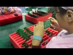
Photoes of this prototype development high-mix low-volume production SMT PCB Assembly