
Add to Cart
8-layer FPC + SMT + TEST + DIP, SMT FPC Service, rigid flex FPC manufacturers, flexible printed FPC, multilayer FPC, flexible FPC
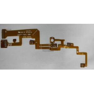
Product Description
Specifications
Our professional engineering team can put your project into
production in a short time. Sample pictures and
BOM are needed to make customized products.Also we can supply for
the copy of the FPC and FPCA, so you
just sent me the enquiry is ok, we can do what you need to do!
We can supply CAD and Pro-E designed precision moulds. Moulds can
be designed and manufactured
according to customers' requests or samples. Plastic injection
processing available.
Purchasing the electronic components for you to the production of
the FPCA
We have advanced equipment for through-hole and SMT DIP COB cable
Assembly
Product Details
PCB capability and services:
PCB, FPC process production capability
| Technical ltem | MassProduct | Advanced Technology | |||||
| 2016 | 2017 | 2018 | |||||
| Max.Layer Count | 26L | 36L | 80L | ||||
| Through-hole plate | 2~45L | 2~60L | 2~80L | ||||
| Max.PCBSize(in) | 24*52" | 25*62" | 25*78.75" | ||||
| The layer number of FPC | 1~36L | 1~50L | 1~60L | ||||
| Max.PCBSize(in) | 9.8"*196" | 9.8"*196" | 10"*196"Reel to reel | ||||
| Layeredplatelayer | 2~12L | 2~18L | 2~26L | ||||
| Max.PCBSize(in) | 9"*48" | 9"*52" | 9"*62" | ||||
| Combination of hard and soft layers | 3~26L | 3~30L | 3~50L | ||||
| Interconnect HDI | 5+X+5Interconnect HDI | 7+X+7Interconnect HDI | 8+X+8,Interconnect HDI | ||||
| HDI PCB | 4~45L | 4~60L | 4~80L | ||||
| Interconnect HDI | 3+20+3 | 4+X+4Interconnect HDI | 4+X+4,Interconnect HDI | ||||
| Max.PCBSize(in) | 24"*43" | 24"*49" | 25"*52" | ||||
| Material | FR-4 Rogers | FR-4 Rogers | FR-4 Rogers | ||||
| Base material | Halogenfree,LowDK | Halogenfree,LowDK | Halogenfree,LowDK | ||||
| Build-up Material | FR-4 | FR-4 | FR-4 | ||||
| BOard,Thickness(mm) | Min.12L(mm) | 0.43 | 0.42~8.0mm | 0.38~10.0mm | |||
| Min.16L(mm) | 0.53 | 1.60~8.0mm | 0.45~10.0mm | ||||
| Min.18L(mm) | 0.63 | 2.0~8.0 | 0.51~10.0mm | ||||
| Min.52L(mm) | 0.8 | 2.50~8.0mm | 0.65~10.0mm | ||||
| MAX(mm) | 3.5 | 10.0mm | 10.0mm | ||||
| Min.CoreThickness um(mil) | 254"(10.0) | 254"(10.0) | 0.10~254(10.0mm) | ||||
| Min.Build up Dielectric | 38(1.5) | 32(1.3) | 25(1.0) | ||||
| BaseCopperWeight | Inner Layer | 4/1-8 OZ | 4/1-15 OZ | 4/1-0.30mm | |||
| Out Layer | 4/1-10 OZ | 4/1-15 OZ | 4/1-30 OZ | ||||
| Gold thick | 1~40u" | 1~60u" | 1~120u" | ||||
| Nithick | 76~127u" | 76~200u" | 1~250u" | ||||
| Min.HOle/Land um(mil) | 150/300(6/12) | 100/200(4/8) | 100/200(4/8) | ||||
| Min.Laser via/landum(mil) | 60/170(2.4/6.8) | 50/150(2/6) | 50/150(2/6) | ||||
| Min. IVH,Hole size/landum(mil) | 150/300(6/12) | 100/200(4/8) | 100/200(4/8) | ||||
| DieletricThickness | 38(1.5) | 32(1.3) | 32(1.3) | ||||
| 125(5) | 125(5) | 125(5) | |||||
| SKipvia | Yes | Yes | Yes | ||||
| viaoNhie(laserviaon BuriedPTH) | Yes | Yes | Yes | ||||
| Laser Hole Filling | Yes | Yes | Yes | ||||
| Technicalltem | Mass Product | Advanced Technolgy | |||||
| 2017year | 2018year | 2019year | |||||
| Drill hole depth ratio | ThroughHole | 2017year | .40:1 | .40:1 | |||
| Aspet Ratio | Micro Via | .35:1 | 1.2:1 | 1.2:1 | |||
| Copper Filling Dimple Size um(Mil) | 10(0.4) | 10(0.4) | 10(0.4) | ||||
| Min.LineWidth&space | lnner Layer um(mil) | 45/45(1.8/1.8) | 38/38(1.5/1.5) | 38/38(1.5/1.5) | |||
| Plated Layer um(mil) | 45/45(1.8/1.8) | 38/38(1.5/1.5) | 38/38(1.5/1.5) | ||||
| BGAPitch mm(Mil) | 0.3 | 0.3 | 0.3 | ||||
| Min.PTH Hole ring um(mil) | 75(3mil) | 62.5(2.5mil) | 62.5(2.5mil) | ||||
| Line Width Control | ∠2.5MIL | ±0.50 | ±0.50 | ±0.50 | |||
| 2.5Mil≤L/W∠4mil | ±0.50 | ±0.50 | ±0.50 | ||||
| ≦3mil | ±0.60 | ±0.60 | ±0.60 | ||||
| Laminated structure | Layer by layer | 3+N+3 | 4+N+4 | 5+N+5 | |||
| Sequential Build-up | 20L Any Layer | 36L Any Layer | 52L Any Layer | ||||
| Multi-layer overlay | N+N | N+N | N+N | ||||
| N+X+N | N+X+N | N+X+N | |||||
| sequential Lamination | 2+(N+X+N)+2 | 2+(N+X+N)+2 | 2+(N+X+N)+2 | ||||
| Soft and hard bonding | 2+(N+X+N)+2 | 2+(N+X+N)+2 | 2+(N+X+N)+2 | ||||
| PTH filling process | PTH resin plug hole + plating fill Electroplated hole/copper plug hole | PTH resin plug hole + plating fill Electroplated hole/copper plug hole | PTH resin plug hole + plating fill Electroplated hole/copper plug hole | ||||
Detailed Specification of PCB Manufacturing
| 1 | layer | 1-30 layer |
| 2 | Material | CEM-1, CEM-3 FR-4, FR-4 High TG, Polyimide, Aluminum-based material. |
| 3 | Board thickness | 0.2mm-6mm |
| 4 | Max.finished board size | 800*508mm |
| 5 | Min.drilled hole size | 0.25mm |
| 6 | min.line width | 0.075mm(3mil) |
| 7 | min.line spacing | 0.075mm(3mil) |
| 8 | Surface finish | HAL, HAL Lead free,Immersion Gold/ Silver/Tin, Hard Gold, OSP |
| 9 | Copper thickness | 0.5-4.0oz |
| 10 | Solder mask color | green/black/white/red/blue/yellow |
| 11 | Inner packing | Vacuum packing,Plastic bag |
| 12 | Outer packing | standard carton packing |
| 13 | Hole tolerance | PTH:±0.076,NTPH:±0.05 |
| 14 | Certificate | UL,ISO9001,ISO14001,ROHS,TS16949 |
| 15 | Profiling punching | Routing,V-CUT,Beveling |
PCB Assembly services:
Automatic Pick & Place
Component Placement as Small as 0201
Fine Pitch QEP - BGA
Automatic Optical Inspection
Through-hole Assembly
Wave Soldering
Hand Assembly and Soldering
Material Sourcing
IC pre-programming / Burning on-line
Function testing as requested
Aging test for LED and Power boards
Complete unit assembly (which including plastics, metal box, Coil,
cable assembly etc)
Packing design
Conformal coating
Both dip-coating and vertical spray coating is available.
Protecting non-conductive dielectric layer that is
applied onto the printed circuit board assembly to protect the electronic assembly from damage due to
contamination, salt spray, moisture, fungus, dust and corrosion caused by harsh or extreme environments.
When coated, it is clearly visible as a clear and shiny material.
Complete box build
Complete 'Box Build' solutions including materials management of
all components, electromechanical parts,
plastics, casings and print & packaging material
Testing Methods
AOI Testing
· Checks for solder paste
· Checks for components down to 0201"
· Checks for missing components, offset, incorrect parts, polarity
X-Ray Inspection
X-Ray provides high-resolution inspection of:
· BGAs
· Bare boards
In-Circuit Testing
In-Circuit Testing is commonly used in conjunction with AOI
minimizing functional defects caused by
component problems.
· Power-up Test
· Advanced Function Test
· Flash Device Programming
· Functional testing
Detailed Specification of Pcb Assembly
| 1 | Type of Assembly | SMT and Thru-hole |
| 2 | Solder Type | Water Soluble Solder Paste,Leaded and Lead-Free |
| 3 | Components | Passives Down to 0201 Size |
| BGA and VFBGA | ||
| Leadless Chip Carries/CSP | ||
| Double-Sided SMT Assembly | ||
| Fine Pitch to 08 Mils | ||
| BGA Repair and Reball | ||
| Part Removal and Replacement-Same Day Service | ||
| 3 | Bare Board Size | Smallest:0.25x0.25 Inches |
| Largest:20x20 Inches | ||
| 4 | File Formats | Bill of Materials |
| Gerber Files | ||
| Pick-N-Place File(XYRS) | ||
| 5 | Type of Service | Turn-Key,Partial Turn-Key or Consignment |
| 6 | Component Packaging | Cut Tape |
| Tube | ||
| Reels | ||
| Loose Parts | ||
| 7 | Turn Time | 15 to 20 days |
| 8 | Testing | AOI inspection |
| X-Ray inspection | ||
| In-Circuit testing | ||
| Functional test |
FAQ:
Q: What files do you use in FPC fabrication?
A: Gerber or Eagle, BOM listing, X, Y sitting report, PNP and Components Position
Q: Is it possible you could offer sample?
A: Yes, we can custom you sample to test before mass production
Q: When will I get the quotation after sent Gerber, BOM and test procedure?
A: Within 6-48hours for FPC quotation and around 24-48 hours for FPCA quotation.
Q: According to the difficulty of high-layer boards, How can I know the process of my FPC production?
A: 7-35days for FPC production and components purchasing, and 14-20days for FPC assembly and Testing
Q: How can I make sure the quality of my FPC?
A: We ensure that each piece of FPC, FPCA products work well before shipping. We'll test all of them according to your test procedure.


