
Add to Cart
2inch GaN substrates template,GaN wafer for LeD,semiconducting Gallium Nitride Wafer for ld,GaN template, mocvd GaN Wafer,Free-standing GaN Substrates by Customized size,small size GaN wafer for LED, mocvd Gallium Nitride wafer 10x10mm,5x5mm, 10x5mm GaN wafer,Non-Polar Freestanding GaN Substrates(a-plane and m-plane)
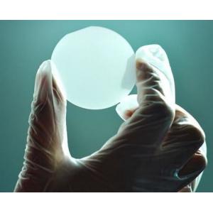
GaN Wafer Characteristic
| Product | Gallium nitride (GaN) substrates | ||||||||||||||
| Product Description: | Saphhire GaN template is presented Epitxial hydride vapor phase epitaxy (HVPE) method. In the HVPE process, the acid produced by the reaction GaCl, which is in turn reacted with ammonia to produce gallium nitride melt. Epitaxial GaN template is a cost-effective way to replace gallium nitride single crystal substrate. | ||||||||||||||
| Technical parameters: |
| ||||||||||||||
| Specifications: | GaN epitaxial film (C Plane), N-type, 2 "* 30 microns, sapphire; GaN epitaxial film (C Plane), N-type, 2 "* 5 microns sapphire; GaN epitaxial film (R Plane), N-type, 2 "* 5 microns sapphire; GaN epitaxial film (M Plane), N-type, 2 "* 5 microns sapphire. AL2O3 + GaN film (N-type doped Si); AL2O3 + GaN film (P-type doped Mg) Note: according to customer demand special plug orientation and size. | ||||||||||||||
| Standard Packaging: | 1000 clean room, 100 clean bag or single box packaging |
Application
GaN can be used in many areas such as LED display, High-energy
Detection and Imaging,
Laser Projection Display, Power Device, etc.
Specifications:
| Non-Polar Freestanding GaN Substrates(a-plane and m-plane) | ||
| Item | GaN-FS-a | GaN-FS-m |
| Dimensions | 5.0mm×5.5mm | |
| 5.0mm×10.0mm | ||
| 5.0mm×20.0mm | ||
| Customized Size | ||
| Thickness | 350 ± 25 µm | |
| Orientation | a-plane ± 1° | m-plane ± 1° |
| TTV | ≤15 µm | |
| BOW | ≤20 µm | |
| Conduction Type | N-type | |
| Resistivity(300K) | < 0.5 Ω·cm | |
| Dislocation Density | Less than 5x106 cm-2 | |
| Useable Surface Area | > 90% | |
| Polishing | Front Surface: Ra < 0.2nm. Epi-ready polished | |
| Back Surface: Fine ground | ||
| Package | Packaged in a class 100 clean room environment, in single wafer containers, under a nitrogen atmosphere. | |
Q&A
Q:What is a GaN wafer?
A:A GaN wafer (gallium nitride wafer) is a thin, flat substrate made from gallium nitride, a wide-bandgap semiconductor material that is widely used in high-performance electronics. GaN wafers are the foundation for manufacturing electronic devices, particularly for applications requiring high power, high frequency, and high efficiency. This material is especially important in industries such as power electronics, telecommunications, and LED lighting.
Q:Why is GaN better than silicon?
A:GaN (gallium nitride) is better than silicon in many high-performance applications due to its wide bandgap (3.4 eV compared to silicon's 1.1 eV), enabling GaN devices to operate at higher voltages, temperatures, and frequencies. GaN's high efficiency leads to lower heat generation and reduced energy loss, making it ideal for power electronics, fast-charging systems, and high-frequency applications. Additionally, GaN has better thermal conductivity, allowing devices to run more efficiently in demanding conditions. As a result, GaN-based devices are more compact, energy-efficient, and reliable than their silicon counterparts.
Key words:#GaN #GalliumNitride #PowerElectronics #HighPerformance #Efficiency #LED #LaserProjection #EnergyEfficientLighting #HighFrequencyDevices #NonPolarGaN #FreestandingGaN #GaNSubstrates #MOCVD

