diameter 150mm 8inch 4inch 6inch Silicon-based AlN templates 500nm
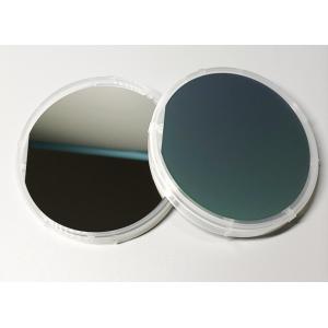
AlN film on silicon substrate
Applications of AlN template
Silicon-based semiconductor technology has reached its limits and
could not satisfy the requirements of future
electronic devices. As a typical kind of 3rd/4th-generation
semiconductor material, aluminum nitride (AlN) has
superior physical and chemical properties such as wide bandgap,
high thermal conductivity, high breakdown filed,
high electronic mobility and corrosion/radiation resistance, and is
a perfect substrate for optoelectronic devices,
radio frequency (RF) devices, high-power/high-frequency electronic
devices, etc.. Particularly, AlN substrate is the
best candidate for UV-LED, UV detectors, UV lasers, 5G
high-power/high-frequency RF devices and 5G SAW/BAW
devices, which could widely be used in environmental protection,
electronics, wireless communications, printing,
biology, healthcare, military and other fields, such as UV
purification/sterilization, UV curing, photocatalysis, coun
terfeit detection, high-density storage, medical phototherapy, drug
discovery, wireless and secure communication,
aerospace/deep-space detection and other fields.
we have developed a serials of proprietary processes and
technologies to fabricate
high-quality AlN templates. At present, Our OEM is the only company
worldwide who can produce 2-6 inch AlN
templates in large-scale industrial production capability with
capacity of 300,000 pieces in 2020 to meet explosive
market demand from UVC-LED, 5G wireless communication, UV detectors
and sensors etc
The factroy is an innovative high-tech company founded in 2016 by
renowned Chinese Overseas professionals from semiconductor
industry.
they focus its core business on development and commercialization
of 3rd/4th-generation ultra-wide bandgap semiconductor AlN
substrates,
AlN templates, fully automatic PVT growth reactors and related
products and services for various high-tech industries.
it has been recognized as a global leader in this field. Our core
products are key strategy materials listed in “Made in China ".
they have developed a serials of proprietary technologies and
the-state-of-the art PVT growth reactors and facilities to
fabricate different sizes of high-quality single crystalline AlN
wafers, AlN temlpates. We are one of the few world-leading
high-tech companies who own full AlN fabrication capa
bilities to produce high-quality AlN boules and wafers, and provide
professional services and turn-key solutions to our customers,
arranged from the growth reactor and hotzone design, modeling and
simulation, process design and optimization, crystal growth,
wafering and material characterization. Up to April 2019, they have
applied more than 27 patents (including PCT).
Specification
Characteristic Specification
- Model UTI-AlN-150S
- Conductivity Type C-plane of Si single crystal wafer
- Resistivity (Ω) >5000
- AlN structure Wurtzite
- Diameter (inch) 6inch
- Substrate thickness (µm) 625 ± 15
- AlN Film thickness (µm) 500nm
- Orientation C-axis [0001] +/- 0.2°
- Usable Area ≥95%
- Cracks None
- FWHM-2θXRD@(0002) ≤0.22°
- FWHM-HRXRD@(0002) ≤1.5°
- Surface Roughness [5×5µm] (nm) RMS≤6.0
- TTV (µm) ≤7
- Bow (µm) ≤40
- Warp (µm) -30~30
- Note: These characterization results may vary slightly depending on
the equipments and/or software employed
| Crystal structure | Wurtzite |
| Lattice constant (Å) | a=3.112, c=4.982 |
| Conduction band type | Direct bandgap |
| Density (g/cm3) | 3.23 |
| Surface microhardness (Knoop test) | 800 |
| Melting point (℃) | 2750 (10-100 bar in N2) |
| Thermal conductivity (W/m·K) | 320 |
| Band gap energy (eV) | 6.28 |
| Electron mobility (V·s/cm2) | 1100 |
| Electric breakdown field (MV/cm) | 11.7 |