Product Details
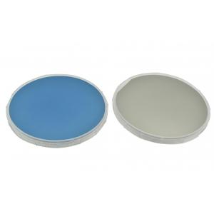
2INCH dia50.8mm Ga doped Ge substrate 4inch N-type 500um Ge wafers
Ge wafer for microelectronic application
N type, Sb doped Ge wafer |
N type,undoped Ge wafer |
P type,Ga doped Ge wafer |
Available size:2”-6” |
Available orientation: (100),(111),or custom specs. |
Available grade: IR grade, electronic grade and cell grade |
Resistivity: |
N - type : 0.007-30 ohm-cm |
| P - type : 0.001-30 ohm-cm |
| Undoped : >=30 ohm-cm |
Surface: as-cut, single side polished, double side polished Ge wafer for optical grade: | SL.No | Material Specifications: | | | 1 | Crystalline Form : | Polycrystalline | | 2 | Conductivity Type : | n-type | | 3 | Absorption Coefficient, at 25°C | 0.035cm-1 max @10.6µm | | 4 | Typical Resistivity : | 3-40 ohm-cm | | 5 | Density : | 5.3 g/cc | | 6 | Mohs Hardness : | 6.3 | | 7 | Oxygen Content : | < 0.03 ppm | | 8 | Holes and Inclusions: | <0.05 mm | | 9 | Poisson Ratio : | 0.278 | | 10 | Youngs Modulus (E) : | 100 Gpa | | | | | SL.No | Optical Properties: | | | 1 | dn/dt from 250-350 K : | 4 X 10⁻⁴ K-1 | | 2 | Transmission at 25°C @10.6 µm wavelength | | | | for uncoated sample of thickness 10mm : | Max. 47% or more | | 3 | Refractive Index @ 10.8 µm : | 4.00372471±0.0005 | | | | SL.No | Thermal Properties | | | 1 | Melting Point (K) : | 1210.4 | | 2 | Heat Capacity @ 300K (J/kg.K): | 322 | | 3 | Thermal Conductivity @293 K : | 59 Wm-1 K-1 | | 4 | Coefficient Thermal Expansion @ (20°C) (10-6 K): | 5.8 |
|
dia25.4mm Ge windows Single Crystal Germanium Ge Wafer for
Semiconductor device
ZMKJ is a worldwide supplier of single crystal Germanium lens and
single crystal Ge ingot , we have a strong advantage in providing
single crystal wafer to micro-electronics and opto-electronics
industry in diameter range from 2 inch to 6inch .
Ge wafer is an elemental and popular semiconductor material , due
to its excellent crystallographic properties and unique electric
properties , Ge wafer is widly used in Sensor , Solar cell and
Infrared optics applications .
We can provide low dislocation and epi ready Ge wafers to meet your
unique requirement. Ge wafer is produced as per semiconductor,with
a good quality control system , ZMKJ Is dedicated to providing
clean and high quality Ge wafer products .
we can offers both electronics grade and IR grade Ge wafer , please
contact us for more Ge product information.
In the range of 2-12 μm, germanium is the most commonly used
material for the production of spherical lenses and windows for
high efficiency infrared in imaging system. Germanium has a high
refractive index (about 4.0 through 2-14μm band), usually do not
need to be modified due to its low chromatic aberration in low
power imaging systems.
Single Crystal Germanium Wafer Capability
we can offer both electronics grade and IR grade Ge wafer and Ge
ingot , please contact us for more Ge product information .| Conductivity | Dopant | Resistivity
( ohm-cm ) | Wafer Size |
|---|
| NA | Undoped | >= 30 | Up to 4 inch |
| N type | Sb | 0.001 ~ 30 | Up to 4 inch |
| P type | Ga | 0.001 ~ 30 | Up to 4 inch |
Q: Do you provide samples? Is it free or charged?
· We'd like to supply samples for free if we have it in stock, but we
don't pay freight.
Q: How long is your delivery time?
· Regarding inventory, it is 3 working days;
· For customized one, it's about 15-25 working days, depended on
exact quantity and order date.
Q: Is it possible to customize special lens?
· Yes, to customize special optical element and coating are available
here.
Q: How to pay?
· T/T, Alibaba online assurance payment, MoneyGram, West Union,
Paypal and so on.
Q: How to ensure the safety of payment?
· ZMKJ is a reliable supplier , reputation and quality is life of our
company, and we support Alibaba Trade Assurance.
Q: How do you ship goods?
· Low value sample: EUB, E Express of China Post, which is cheap;
· Light weight parcel: DHL, FedEx, TNT, UPS, EMS, SF Express, China
Post;
· Heavy cargo: by air or by sea, ship on pallet.
Our company enjoy a considerable discount owing to long-term
cooperation with courier company.
Company Profile
SHANGHAI FAMOUS TRADE CO.,LTD. locates in the city of Shanghai,
Which is the best city of China, and our factory is founded in Wuxi
city in 2014.
We specialize in processing a varity of materials into wafers,
substrates and custiomized optical glass parts.components widely
used in electronics, optics, optoelectronics and many other fields.
We also have been working closely with many domestic and oversea
universities, research institutions and companies, provide
customized products and services for their R&D projects.
It's our vision to maintaining a good relationship of cooperation
with our all customers by our good reputatiaons.