
Add to Cart
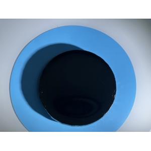
2inch 3inch 4inch 6inch SiC Ingot and substrate 4H-N/Semi Type SiC Ingots Industrial Dummy2inch/3inch/4inch/6inch 6H-N/4H-SEMI/ 4H-N SIC ingots/High purity 4H-N 4inch 6inch dia 150mm silicon carbide single crystal (sic) substrates wafers, sic crystal ingots sic semiconductor substrates, Silicon Carbide crystal Wafer/ Customzied as-cut sic wafers
Silicon carbide (SiC), also known as carborundum, is a semiconductor containing silicon and carbon with chemical formula SiC. SiC is used in semiconductor electronics devices that operate at high temperatures or high voltages, or both.SiC is also one of the important LED components, it is a popular substrate for growing GaN devices, and it also serves as a heat spreader in high-power LEDs.
| Growth | PVT | Unit | |||
| Diameter | 50.8 ± 0.5 | 76.2 ± 0.5 | 100.0 ± 0.5 | 150 ± 0.5 | |
| Polytype | 4H / 6H | 4H | 4H | 4H | mm |
| Surface Orientation | 0.0˚/4.0˚/8.0˚ ± 0.5˚ | 4.0˚ ± 0.5˚ | 4.0˚ ± 0.5˚ | 4.0˚ ± 0.5˚ | degree |
| Type | N - type | ||||
| Thickness | 5~10 / 10~15 / > 15 | mm | |||
| Primary Flat | (10-10) ± 5.0˚ | degree | |||
| Primary Length | 15.9 ± 2.0 | 22.0 ± 3.5 | 32.5 ± 2.0 | 47.5 ± 2.5 | mm |
| Secondary Flat | 90˚ CCW from orientation ± 5.0˚ | degree | |||
| Secondary Length | 8.0 ± 2.0 | 11.2 ± 2.0 | 18.0 ± 2.0 | None | mm |
| Grade | Research / Dummy | ||||
| Property | 4H-SiC, Single Crystal | 6H-SiC, Single Crystal |
| Lattice Parameters | a=3.076 Å c=10.053 Å | a=3.073 Å c=15.117 Å |
| Stacking Sequence | ABCB | ABCACB |
| Mohs Hardness | ≈9.2 | ≈9.2 |
| Density | 3.21 g/cm3 | 3.21 g/cm3 |
| Therm. Expansion Coefficient | 4-5×10⁻⁶/K | 4-5×10⁻⁶/K |
| Refraction Index @750nm | no = 2.61 ne = 2.66 | no = 2.60 ne = 2.65 |
| Dielectric Constant | c~9.66 | c~9.66 |
| Thermal Conductivity (N-type, 0.02 ohm.cm) | a~4.2 W/cm·K@298K c~3.7 W/cm·K@298K | |
| Thermal Conductivity (Semi-insulating) | a~4.9 W/cm·K@298K c~3.9 W/cm·K@298K | a~4.6 W/cm·K@298K c~3.2 W/cm·K@298K |
| Band-gap | 3.23 eV | 3.02 eV |
| Break-Down Electrical Field | 3-5×10⁶V/cm | 3-5×10⁶V/cm |
| Saturation Drift Velocity | 2.0×10⁵m/s | 2.0×10⁵m/s |
High purity 4inch diameter Silicon Carbide (SiC) Substrate Specification
Silicon carbide wafer is a kind of basic material widely evaluated in semiconductor device manufacturing. It has the characteristics of high hardness, high heat resistance, high chemical stability and high temperature resistance. The following are some of the main applications of silicon carbide wafers in semiconductor device manufacturing:
Power semiconductor device manufacturing: Silicon carbide wafers are widely used in power semiconductor device manufacturing, such as IGBT, MOSFET, differential and so on. Because the silicon carbide high breakdown has the characteristics of resistance strength, high thermal conductivity and low on-resistance, it can greatly improve the performance of power semiconductor devices, such as reducing the switching loss and improving the switching speed.
Optoelectronic device manufacturing: Silicon carbide wafers are also used to manufacture optoelectronic devices, such as leds, laser attenuation, etc. Silicon carbide wafers have optical brightness and high temperature resistance, giving them advantages in the manufacture of high temperature leds and high power lasers.
Wireless communication device manufacturing: silicon carbide devices can also be used to manufacture wireless communication devices, such as SIC MESFET, SIC HEMT, etc. Silicon carbide devices have the characteristics of high electron mobility and high microwave frequency response speed, which has potential application value in high frequency devices.
Other applications: Silicon carbide wafers can also be used to manufacture sensors, thermoelectric devices, solar cells and other fields. The high hardness and chemical stability of silicon carbide wafers have potential applications in the manufacture of wear-resistant and corrosion-resistant components.
4H-N Type / High Purity SiC wafer/ingots 2 inch 4H N-Type SiC wafer/ingots 3 inch 4H N-Type SiC wafer 4 inch 4H N-Type SiC wafer/ingots 6 inch 4H N-Type SiC wafer/ingots | 4H Semi-insulating / High Purity SiC wafer 2 inch 4H Semi-insulating SiC wafer 3 inch 4H Semi-insulating SiC wafer 4 inch 4H Semi-insulating SiC wafer 6 inch 4H Semi-insulating SiC wafer |
6H N-Type SiC wafer 2 inch 6H N-Type SiC wafer/ingot | Customzied size for 2-6inch |
FAQ:
Q: What's the way of shipping and cost?
A:(1) We accept DHL, Fedex, EMS etc.
(2) it is fine If you have your own express account ,If not,we could help you ship them and
Freight is in accordance with the actual settlement.
Q: How to pay?
A: T/T 100% deposit before delivery.
Q: What's your MOQ?
A: (1) For inventory, the MOQ is 1pcs. if 2-5pcs it's better.
(2) For customized commen products, the MOQ is 10pcs up.
Q: What's the delivery time?
A: (1) For the standard products
For inventory: the delivery is 5 workdays after you place the order.
For customized products: the delivery is 2 -4 weeks after you order contact.
Q: Do you have standard products?
A: Our standard products in stock. as like substrates 4inch 0.35mm.

