
Add to Cart
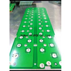
Cu base PCB MCPCB New energy PCB copper pcb board heavy copper pcb copper circuit board
| PCB Type | Material Type | Material Brand | |||||||
| Single side pcb Double side pcb Multilayer pcb Single side pcb | CEM-1 FR-4 Aluminum Copper Ceramic | SY KB IL LianMao HongRen Arlon KingWong VT Laird 5052 Series | |||||||
| The advantage of us | |||||||||
| 1 | We have our own, independent of the wastewater treatment system.Make sure there will be a very big development space and the stability of the production environment in the futurer | ||||||||
| 2 | Flexible operation, can be in the production of small batches.Also can produce large quantities.Can save production quickly. | ||||||||
| 3 | The urgent double sample production for 24 hours, The urgent Multilayer sample production for 48 hours.completely according to customer requirements | ||||||||
| About the Files | |||||||||
| 1 | You have gerber files or PCB files | ||||||||
| 2 | You have PCB samples. send to us the sample. we will help for free copy it | ||||||||
| How to calculate the price | |||||||||
| 1 | For example, your double sided PCB size is 100 mm * 200 mm wide, long double sided PCB price is $60 a square meters.So the calculation results 100MM*200MM*$60/1000000=$1.2 | ||||||||
| 1 inch=25.4mm | |||||||||
| About the transportation. | |||||||||
| All the quotation does not include the transportation cost | |||||||||
| 1 | You find a freight forwarding company to help you, When we finished the PCB ,We wiill send to your forwarder company directly .You directly to the transport charges paid to forwarder company | ||||||||
| 2 | We help you responsible for transport, freight included in the price.According to how much money a kilogram computation. | ||||||||
| 3 | In order to save costs.The best is you have familiar forwarder company | ||||||||
Processing Capability
| Material Type: FR4/Aluminum/Ceramic/CEM-1/Copper/polytef | Cooper thickness: 0.5-12OZ | |||||||||||||
| Board Thickness: 0.2-6.0mm | Min hole size: 0.25mm( finished hole size) | |||||||||||||
| Min Line Width/spacing:0.08mm | Drilling accuracy:+/-0.05 | |||||||||||||
| Max working size:520*620mm(21.25x24.5inch) | Min Inner layer thickness:0.1mm | |||||||||||||
| Min thickness Board for HAL surface finished:0.4mm | Certificate: Rohs, Iso9001, UL(in certification) | |||||||||||||
| Min thickness 4 layer: 0.4mm | Min thickness 6 layer:0.6mm | |||||||||||||
| Min/Max layer count : 1/20 | Lamination evenness :+/-0.05mm | |||||||||||||
| Min SMD Pitch : 0.125mm | Min Dam Between Fine Pitch: >0.1mm | |||||||||||||
| Layer to Layer registration:<0.1mm | Impedance control:+/-5% | |||||||||||||
| Differential impedance:+/-10% | Board bow/twist tolerance:<0.7% | |||||||||||||
| Plating spect ratio: <8:1 | Plating COV: <10% | |||||||||||||
| Surface Finished: LF-HASL ,Immersion Gold/Tin/Silver ./Plating Gold/OSP, | PTH backlight : 9-9.5 level | |||||||||||||
| Solder Mask:Green , Red, Blue,White, Black,Yellow. | Plating extensibility:>15% | |||||||||||||
Copper clad aluminum plate has been widely used in LED lights,
microelectronics and other fields.It has the incomparable advantage over traditional ceramic
substrates:
(1) can be greatly reduced the quality of the power module, meet
the needs of lightweight development module, and the traditional
module of heat dissipation copper plate and ceramic substrate
density is bigger, heavier quality;
(2) can make the power module encapsulation easier, save ceramic
substrate and copper cooling plate screen printing process, such as
the production cycle is shorten, conducive to module automation
production.
(3) has good thermal conductivity and dielectric properties;
(4) copper clad aluminum plate than the cooling copper plate and
DBC ceramic substrates are much lower price, can make the power
module of the production cost greatly reduced.


