
Add to Cart
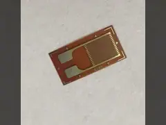
Description Semiconductor strain gauge is used for making sensor the used elastic element of stress analysis of commonly. Sensitive coefficient less mechanical hysteresis and wide range of resistance and low transverse effect etc. It can be used to measure the stress distribution and components...
Description
Semiconductor strain gauge is used for making sensor the used
elastic element of stress analysis of commonly. Sensitive
coefficient less mechanical hysteresis and wide range of resistance
and low transverse effect etc. It can be used to measure the stress
distribution and components of force - electrical conversion.
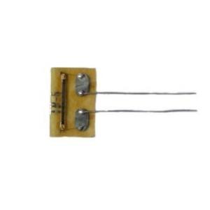
For machinery aviation ships bridges engineering structures such as
the static measurement more complex stress analysis it can also be
used to fulfill nonlinear compensation of foil sensor. The company
not only can product various regular strain gauge and will provide
you with the different requirements of the product such as
temperature no basal type.
Features
nonlinear compensation of foil sensor
machinery aviation ships bridges
Micro pressure sensor
Technical Data
Semiconductor strain gauge characteristics
Model Number | SYP-15 | SYP-30 | SYP-60 | SYP-120 | SYP-350 | SYP-600 | SYP-1000 |
Gage resistance() | 15±5% | 30±5% | 60±5% | 120±5% | 350±5% | 600±5% | 1000±5% |
Code | B,C | B,C | B,C | A,B,C | B,C | C | C,D |
construction | 0,F2,F3,F4,F5 | 0,F2,F3,F4,F5 | 0,F2,F3,F4,F5 | 0,F2,F3,F4,F5 | 0,F2,F3,F4,F5 | 0,F2,F3,F4,F5 | C:0,F2,F3,F4,F5 |
K | 100 | 100 | 120 | A:150 | 150 | 200 | C:200 |
TCR (%/℃) | 0.10 | 0.10 | 0.15 | 0.13 | 0.30 | 0.45 | C:0.40 |
TCGF (%/℃) | -0.12 | -0.12 | -0.18 | A:-0.35 | -0.35 | -0.48 | C:-0.48 |
maximum operating current(mA) | 50 | 50 | 50 | A:20 | 30 | 20 | 20 |
Strain limits(m) | 5000 | 5000 | 5000 | 5000 | 5000 | 5000 | 5000 |
Dimension
Semiconductor strain gauge (without substrate) | |||
Code | configuration | size (mm) | Gage resistance |
A | 1.27×0.22×(0.020~0.030) | 15,30,60,120 | |
B | 3.8×0.22×(0.020~0.030) | 15,30,60,120,350 | |
C | 4.7×0.22×0.02 | 15,30,60,120,350,600,1000 | |
D | 6×0.22×0.02 | 1000 | |
① The copper wire length of Semiconductor strain gage (without
substrate) is shorter than 6mm; | |||
Example: SYP 1000 C F3
explicate: P-Si Semiconductor strain gage
resistance: 1000;
K: 200;
Silicon: 4.7×0.22×0.02;
Substrate size: 7×4
Note: if there are other requirements or the size of the substrate or
the silicon strip must be specified in the contract
Miniature Load Cells SL-01
Weighing Module SDK-01
Postal Bench Scales
Truck Scale Remote Scoreboard
Shear Beam Load Cells DB-07
Single Point Load Cells SPA-49