
Add to Cart
Surface Acoustic Wave Propagation On Piezoelectric Crystal LT LN Wafers
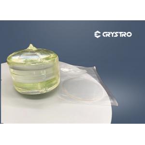
Surface Acoustic Wave Propagation On Piezoelectric LT LN Crystal Wafers
Crystro can customize Surface Acoustic Piezoelectric Wafers including Lithium Niobate,Lithium Tantalate,Quartz Crystal as reuqired
cutting orientation and size,our Piezoelectric Effect crystals are grown by Czochralski method. Max diameter reach 6inch,we can custom size and specs ,rougness<0.5nm.
Dia 3" 4" 6" wafers are all available as per requirement.
Crystro possess Corning Flatmaster 200 Profiler, Laser marking
equipment, AOI and 6-step cleaning line.
Crystro provides:
Basic Properties of LiTaO3:
| Material | Lithium Niobate | Lithium Tantalate | Quartz Crystal |
| Diameter / Size | 3’’, 4’’, 6’’, 8’’ | 3’’, 4’’, 6’’ | 3’’, 4’’, 5’’, 6’’, 8’’ |
| Cut Type | X / Y / Z | X / Y-Z / X-112Y | X / Y / Z |
| 36Y / 64Y/128Y | 28Y / 36Y / 42Y | AT / ST / DT | |
| Surface Finish | Double side polish / Single side polish | ||
| Thickness | 0.25mm / 0.35mm / 0.50mm / 1.00mm / 2.00mm | ||
| TTV | < 5um | ||
| PLTV | >98% (5mm*5mm) | ||
| LTV | < 1.5um | ||
| Bow | -25um < Bow < +25um | ||
| Warp | < 30um | ||
| Roughness | Ra<0.5nm, Ra<1nm | ||
| Curie Temp. | 1142℃ ± 2℃ | 605℃ ± 2℃ | 573℃ |
| Edge Profile | Round Ground, "C" Shape | ||
| Flats | 22±2mm, 32.5±2mm, 47.5±2mm, 57.5±2mm, Notch | ||
| As per request | |||
| Dope with | Er, MgO | Fe | with or without seed |
| Front Side | Roughness Ra<= 10A | ||
| Back Side | Roughness Ra: 0.2--0.7um GC#1000, GC#2000 | ||
| Appearance | No Cracks, saw marks, stains | ||
| Single Domian | Completed Polarization / Reduced | No Stress | |