
Add to Cart
CNSMT Electronic printed circuit board fast delivery led smd pcb board Low Price sample
Quick Detail
Feature
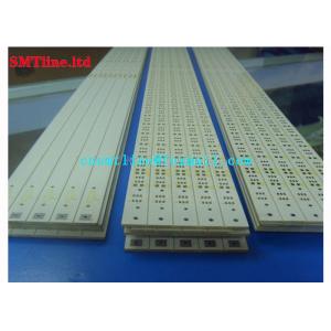
| Product Name: | SMD LED PCB Board |
| Used for: | SMT FACTORY Electronic Circuit Board |
| Warranty: | 1 Year |
| Shipment | by air |
| Delivery Time: | 1-2Days |
| Our Main Market | Whole of the world |
Application
Setting skills
Different points need to be set in different stages of design, and
large grid points can be used for device layout in the layout
stage.
For ICs, non-positioning connectors, and other large devices, 50-
to 100-mil lattice points can be used for layout. For passive small
devices such as resistors, capacitors, and inductors, 25 mil grids
can be used for layout. The accuracy of the large grids facilitates
the alignment of the devices and the aesthetics of the layout.
PCB layout rules:
1. Under normal circumstances, all components should be placed on
the same surface of the circuit board. Only when the top layer
components are too dense, can some devices with limited height and
low heat, such as chip resistor, chip capacitor, and paste Chip ICs
are placed on the bottom layer.
2. Under the premise of guaranteeing electrical performance,
components should be placed on the grid and arranged parallel or
perpendicular to each other, in order to be neat and beautiful.
Under normal circumstances, no overlap of components is allowed;
the arrangement of components should be compact, and the components
should be arranged on the whole surface of the grid. Uniform
distribution, density and consistency.
3. The minimum spacing between adjacent pad patterns of different
components on the circuit board should be above 1MM.
4, from the edge of the circuit board is generally not less than
2MM. The best shape of the circuit board is a rectangle, the aspect
ratio is 3:2 or 4:3. When the circuit board is more than 200MM by
150MM, you should consider the circuit board can withstand
Mechanical strength.
Layout skills
In the layout design of the PCB, it is necessary to analyze the
elements of the circuit board. According to the function layout
design, when the layout of all components of the circuit, it is
necessary to comply with the following principles:
1. Arrange the positions of each functional circuit unit according
to the circuit's flow, so that the layout is convenient for signal
circulation and the signal is kept in the same direction as
possible.
2. Focus on the core components of each functional unit and lay out
around him. The components should be evenly, integrally, and
compactly arranged on the PCB to minimize and shorten the leads and
connections between the components.
3, in the work of high-frequency circuits, to consider the
distribution parameters between components. The general circuit
should arrange parallel components as much as possible, which is
not only beautiful, but also easy to install welding, easy mass
production.


