
Add to Cart
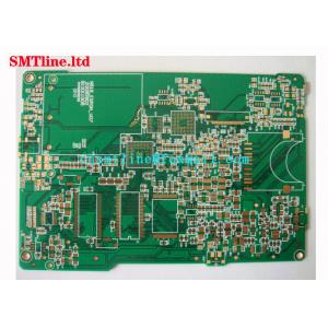
CNSMT bluetooth audio receiver pcb board Component Electronic OEM aluminium pcb boards
Quick Detail
Feature
| Product Name: | SMD LED PCB Board |
| Used for: | SMT FACTORY Electronic Circuit Board |
| Warranty: | 1 Year |
| Shipment | by air |
| Delivery Time: | 1-2Days |
| Our Main Market | Whole of the world |
Application
Layout check
1, the board size and drawings require processing dimensions are in
line.
2. Whether the layout of the components is balanced, neatly
arranged, or whether they have been completely finished.
3, there is no conflict at all levels. Such as the components, the
frame, the level of need for private printing is reasonable.
3, the commonly used components are easy to use. Such as switches,
plug-in boards, equipment that must be replaced frequently, etc.
4. Is the distance between the thermal components and heating
components reasonable?
5, heat dissipation is good.
6. Whether the line interference problem needs to be considered.
[3]
Specific method editing
Purpose effect
1.1 Standardize design operations, increase production efficiency
and improve product quality.
Scope of application
1.1 XXX company development department VCD Super VCDDVD audio and
other products.
Responsibility
3.1 All electronic engineers, technicians, and computer drafters of
the XXX Development Department.
Qualification training
4.1 There is a basis for electronic technology;
4.2 Basic knowledge of computer operations;
4.3 Familiar with the use of computer PCB drawing software.
Work guidance
5.1 Minimum Line Width of Copper Foil: 0.1MM, Panel 0.2MM Minimum
1.0MM for Edge Copper Foil
5.2 Copper foil minimum clearance: 0.1MM, panel: 0.2MM.
5.3 The minimum distance between the copper foil and the edge of
the board is 0.55MM, the minimum distance between the component and
the board edge is 5.0MM, and the minimum distance between the board
and the board edge is 4.0MM.
5.4 The size of the pad of a common through-hole mounting device is
twice the size (diameter) of the pad, and the minimum is 1.5mm for
the double panel, and the minimum is 2.0mm for the single panel.
(2.5mm) If you can not use the round pad, use the round lug welding
Disk, as shown below (if there is a standard library,
The standard component library will prevail
The relationship between the long edge, short edge, and hole of the
pad is:
5.5 Electrolytic capacitor can not touch the heating element, high
power resistance, sensitive resistance, pressure, heat, etc. The
minimum distance between the solution capacitor and the heat sink
is 10.0MM, and the minimum distance between the component and the
heat sink is 2.0MM.
5.6 Large-sized components (such as transformers, electrolytic
capacitors with a diameter of 15.0 mm or more, and sockets with
large currents, etc.) Increase the copper foil and tin area as
shown in the figure below. The area of the shadowed area should
be equal to the area of the pad.
5.7 The screw hole radius 5.0MM cannot have copper foil (required
grounding outside) components. (according to structural drawing
requirements).
5.8 Tin can not have silk oil.
5.9 pad center distance is less than 2.5MM, adjacent pad
surrounding the silk screen oil package, ink width 0.2MM (meeting
0.5MM).
5.10 Jumpers should not be placed underneath the IC or under
components of motors, potentiometers, and other large metal
enclosures.
5.11 In large-area PCB design (above about 500CM2 or more), prevent
the PCB board from bending when passing the soldering tin, and
leave a space of 5 to 10mm wide in the middle of the PCB board to
keep the components (wires) away from the tin furnace. When adding
a layer to prevent the PCB from bending, the shaded area in the
following figure:
5.12 Each transistor must be marked on the silkscreen with legs e,
c, and b.
5.13 Components that need to be soldered after soldering, the
plates must be driven away from the tin position. To the contrary
with the tin, the size of the hole is 0.5mm to 1.0mm as shown
below:
5.14 Pay attention to the design of the double panel, the
components of the metal shell, when the plug is in contact with the
printed board, the top layer of the pad can not be opened, must be
covered with green oil or screen printing oil (such as two feet of
the crystal).


