
Add to Cart
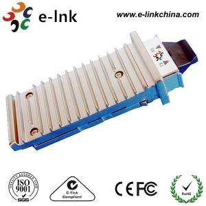
X2 10GBASE-SR SC 850nm 300m SFP Optical Transceiver Module
Features
Applications
Absolute Maximum Ratings
| Parameter | Symbol | Min | Max | Unit | Ref. |
| Storage Ambient Temperature Range | -40 | +85 | °C | non condensing | |
| Powered case Temperature Range | 0 | +70 | °C | non condensing | |
| Adaptable Power Supply (APS) | Vapsense | 0 | 1.5 | V | Voltage @ Pin APS Sense |
| Supply Voltage Range @ 3.3V | Vcc3 | -0.5 | 4.0 | V |
Any stress beyond the maximum ratings can result in permanent damage. The device specifications are guaranteed only under the recommended operating conditions.
Operating Conditions
| Parameter | Symbol | Min | Typical | Max | Unit | |
| Operating Case Temperature | Tc | 0 | +70 | °C | ||
| Power Supply Voltage | VCC3 | 3.14 | 3.3 | 3.47 | V | |
| VAPS | 1.152 | 1.2 | 1.248 | |||
| Power Dissipation | PD | 1.7 | 2.4 | W | ||
Transmitter Characteristics
| Parameter |
Symbol |
Min. |
Typ. |
Max. |
Unit |
Note |
| Operating Range |
|
|
|
300 |
m |
|
| Operating Date Rate | 10.3125 | Gb/s | ||||
| Average Optics Power | Po |
-6.5 |
|
-1 |
dBm | |
| Input Centre Wavelength | λ | 840 | 850 | 860 | nm | |
| Spectral Width | Δλ | 0.4 | 0.45 | dB | ||
| Extinction Ratio |
ER |
3.5 |
|
|
|
|
| Optical Modulation Amplitude |
OMA |
525 |
|
|
µW |
|
| Transmitter and Dispersion Penalty |
TDP |
|
|
3.2 |
dB |
|
Receiver Characteristics
| Parameter |
Symbol |
Min. |
Typ. |
Max. |
Unit |
Note |
| Operating Date Rate | 10.3125 | Gb/s | ||||
| Average Receiver Power | Po |
-9.9 |
|
-1.0 |
dBm | |
| Sensitivity in OMA | OMA0 | -11.1 | dBm | 1 | ||
| Stressed Sensitivity in OMA |
OMAst |
|
|
-7.5 |
dBm |
|
Note :
1. Measured at 10.3125Gb/s,Non-framed PRBS2^31-1,NRZ
XAUI I/O Characteristics
| Parameter | Symbol | Min. | Typ. | Max. | Unit | Note |
| XAUI Date Rate | DR | 3.125 | Gb/s | |||
| XAUI Baud Rate Tolerance | -100 | +100 | ppm | Relative Tolerance | ||
| Differential Input Voltage Swing | 220 | 1600 | mv | 8B/10B Coded Input Signal | ||
| Differential Output Voltage Swing | 800 | 1600 | mVp-p | RLOAD = 100Ω ± 5% | ||
| Differential Input Impedance | 80 | 100 | 120 | Ω | ||
| Total Output Jitter | TJXAUI | 0.35 | UI | no pre-equalization | ||
| Total Deterministic Output Jitter | DJXAUI | 0.17 | UI | no pre-equalization |
Signal Specifications – Electrical
| Parameter | Symbol | Min | Typ | Max | Units |
| 1.2 V CMOS | |||||
| Input High Voltage | VIL(MAX) | - | - | 0.36 | V |
| Input Low Voltage | VIH(MIN) | 0.84 | - | 1.25 | V |
| Capacitance | - | - | 320 | pF | |
| Pull Up Resistance | Rpull | 4.7k | 10k | 22k | ohm |
| MDIO I/O | |||||
| Output Low Voltage | VOL | -0.3 | - | 0.2 | V |
| Output Low Current | IOL | - | - | 4 | mA |
| Input High Voltage | VIH | 0.84 | - | 1.5 | V |
| Input Low Voltage | VIL | -0.3 | - | 0.36 | V |
| Pull-up Supply Voltage | VPULL | 1.14 | 1.2 | 1.26 | |
| Input Capacitance | CIN | - | - | 10 | Pf |
| Load Capacitance | CLOD | - | - | 470 | Pf |
| External Pull-up Resistance | EPULL | 200 | - | - | Ohm |
Pin Definitions
| Pin No | Name | Dir | Function | Notes |
| 1 | GND | Electrical Ground | 1 | |
| 2 | GND | Electrical Ground | 1 | |
| 3 | GND | Electrical Ground | 1 | |
| 4 | 5.0V | Power | 2 | |
| 5 | 3.3V | Power | 2 | |
| 6 | 3.3V | Power | 2 | |
| 7 | APS =1.2V | Adaptive Power Supply | 2 | |
| 8 | APS =1.2V | Adaptive Power Supply | 2 | |
| 9 | LASI |
Open Drain Compatible 10K-22K pull up on host. Logic High: Normal Operation Logic Low: LASI Asserted |
3 | |
| 10 | RESET | I |
Open Drain compatible. 10-22K pull-up on transceiver Logic high = Normal operation Logic low = Reset Minimum reset assert time 1 ms |
3 |
| 11 | VEND SPECIFIC |
Vendor Specific Pin. Leave unconnected when not in use. |
6 | |
| 12 | TX ON/OFF | I |
Open Drain compatible. 10-22K pull-up on transceiver Logic high = Transmitter On (capable) Logic low = Transmitter Off (always) |
3 |
| 13 | RESERVED | Reserved | 3 | |
| 14 | MOD DETECT | O | Pulled low inside module through 1k | |
| 15 | VEND SPECIFIC |
Vendor Specific Pin. Leave unconnected when not in use. |
6 | |
| 16 | VEND SPECIFIC |
Vendor Specific Pin. Leave unconnected when not in use. |
6 | |
| 17 | MDIO | I/O | Management Data IO | 3, 4 |
| 18 | MDC | I | Management Data Clock | 3, 4 |
| 19 | PRTAD4 | I | Port Address Bit 4 (Low = 0) | 3 |
| 20 | PRTAD3 | I | Port Address Bit 3 (Low = 0) | 3 |
| 21 | PRTAD2 | I | Port Address Bit 2 (Low = 0) | 3 |
| 22 | PRTAD1 | I | Port Address Bit 1 (Low = 0) | 3 |
| 23 | PRTAD0 | I | Port Address Bit 0 (Low = 0) | 3 |
| 24 | VEND SPECIFIC |
Vendor Specific Pin. Leave unconnected when not in use. |
6 | |
| 25 | APS SET | Feedback input for APS | ||
| 26 | RESERVED | Reserved for Avalanche Photodiode use. | 6 | |
| 27 | APS SENSE | APS Sense Connection | ||
| 28 | APS =1.2V | Adaptive Power Supply | 2 | |
| 29 | APS =1.2V | Adaptive Power Supply | 2 | |
| 30 | 3.3V | Power | 2 | |
| 31 | 3.3V | Power | 2 | |
| 32 | 5.0V | Power | 2 | |
| 33 | GND | Electrical Ground | 1 | |
| 34 | GND | Electrical Ground | 1 | |
| 35 | GND | Electrical Ground | 1 | |
| 36 | GND | Electrical Ground | 1 | |
| 37 | GND | Electrical Ground | 1 | |
| 38 | RESERVED | Reserved | ||
| 39 | RESERVED | Reserved | ||
| 40 | GND | Electrical Ground | 1 | |
| 41 | RX LANE0+ | O | Module XAUI Output Lane 0+ | 5 |
| 42 | RX LANE0- | O | Module XAUI Output Lane 0- | 5 |
| 43 | GND | Electrical Ground | 1 | |
| 44 | RX LANE1+ | O | Module XAUI Output Lane 1+ | 5 |
| 45 | RX LANE1- | O | Module XAUI Output Lane 1- | 5 |
| 46 | GND | Electrical Ground | 1 | |
| 47 | RX LANE2+ | O | Module XAUI Output Lane 2+ | 5 |
| 48 | RX LANE2- | O | Module XAUI Output Lane 2- | 5 |
| 49 | GND | Electrical Ground | 1 | |
| 50 | RX LANE3+ | O | Module XAUI Output Lane 3+ | 5 |
| 51 | RX LANE3- | O | Module XAUI Output Lane 3- | 5 |
| 52 | GND | Electrical Ground | 1 | |
| 53 | GND | Electrical Ground | 1 | |
| 54 | GND | Electrical Ground | 1 | |
| 55 | TX LANE0+ | I | Module XAUI Input Lane 0+ | 5 |
| 56 | TX LANE0- | I | Module XAUI Input Lane 0- | 5 |
| 57 | GND | Electrical Ground | 1 | |
| 58 | TX LANE1+ | I | Module XAUI Input Lane 1+ | 5 |
| 59 | TX LANE1- | I | Module XAUI Input Lane 1- | 5 |
| 60 | GND | Electrical Ground | 1 | |
| 61 | TX LANE2+ | I | Module XAUI Input Lane 2+ | 5 |
| 62 | TX LANE2- | I | Module XAUI Input Lane 2- | 5 |
| 63 | GND | Electrical Ground | 1 | |
| 64 | TX LANE3+ | I | Module XAUI Input Lane 3+ | 5 |
| 65 | TX LANE3- | I | Module XAUI Input Lane 3- | 5 |
| 66 | GND | Electrical Ground | 1 | |
| 67 | RESERVED | Reserved | ||
| 68 | RESERVED | Reserved | ||
| 69 | GND | Electrical Ground | 1 | |
| 70 | GND | Electrical Ground | 1 |
Notes:
1) Ground connections are common for TX and RX.
2) All connector contacts are rated at 0.5A nominal.
3) 1.2V CMOS compatible.
4) MDIO and MDC timing must comply with IEEE802.3ae, Clause 45.3
5) XAUI output characteristics should comply with IEEE802.3ae Clause 47.
6) Transceivers will be MSA compliant when no signals are present on the vendor specific pins.