Product Details
Multi-layer control board, single and double-sided PCB circuit
board WIFI camera circuit board PCBA development
Essential details
- Model Number:
JIETENG Pcba
- Place of Origin:
Guangdong, China
- Base Material:
CEM-1 pcba circuit board
- Copper Thickness:
1/2OZ 1OZ 2OZ 3OZ
- Min. Hole Size:
0.20mm pcb board
- Min. Line Width:
0.1 mm pcba assembly
- Surface Finishing:
HASL circuit board
- Product name:
PCB/PCBA/Circuit boards
- Application:
Electronics Device pcba
- Item:
Custom Circuit Board
- Board Thickness:
1.8mm 1.2mm pcba board
- Material:
green blue white black pcba board
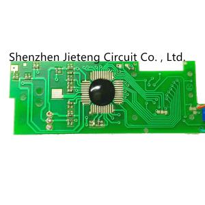
Product Name | shenzhen pcb pcba service manufacture double layer pcb circuit
boards |
Material | FR-4, Hi-Tg FR-4, Lead free Materials (RoHS Compliant) , CEM-3,
CEM-1, Aluminium, High frequency Material (Rogers, Teflon, Taconic) |
Layer No. | 1-30 layers |
Surface finish | HAL, HASL Lead Free, Immersion gold, Gold plating, Gold finger,
immersion silver, immersion Tin, OSP, Carbon ink, |
Board thickness | 0.0075"(0.2mm)-0.125"(3.2mm) |
Certificate | ROHS ISO9001:2000 TS16949 SGS UL |
Special requirements | Buried and blind vias, Impedance control, via plug, BGA soldering
and gold finger |
Files | Gerber, Protel, Powerpcb, Autocad, Cam350, etc |
Company Profile
Shenzhen Jieteng Circuit Co., Ltd. is a one-stop service company
integrating PCB circuit board prototyping, PCBA, and mass
production. The company has engineers with more than 10 years of
experience in this industry, providing customers with constructive
advice on circuit board production to avoid hidden dangers, provide
high-quality PCB circuit board production, and reduce the loss rate
of PCB circuit boards. PCBs procured by customers, as well as
complaint rates and procurement costs, shorten the customer's
procurement cycle. The company's main products include:
double-sided and multi-layer fiberglass PCB,
polytetrafluoroethylene PCB, polyimide flexible board FPC and
aluminum substrate PCB. Products are widely used in high-tech
education fields such as communications, power supply, computer
networks, digital products, industrial control, science and
education, lighting, aerospace, and national defense. Our customers
are all over the world, including the United Kingdom, Russia,
Brazil, Australia, South Korea, etc. We welcome friends from all
walks of life to visit, provide guidance and negotiate business.