Product Details
Factory direct sales of PCB medical equipment HDI blind hole board
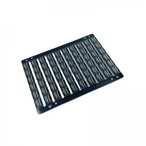
high-precision PCB processing
With Our Professional Departments, We Can Offer:
- PCB Design
- PCB Manufacture: PCB file or Gerber file needed
- PCB PCBA SMD SMT Assembly: Bom list needed
- Electronic Design
- Reverse Engineering - PCB Copy, PCB Clone, IC Decode
- Components Procurement
- PCB PCBA Finished Product Test
- Mass-Production
- Prodcution Contract Manufacturing
- NDA - Non-Disclosure Agreement
Essential details
- Model Number:
K14-026
- Type:
Pcb Manufacture
- Place of Origin:
Guangdong, China
- Brand Name:
TH
- Number of Layers:
1-8 layer
- Base Material:
FR4
- Copper Thickness:
1oz
- Board Thickness:
1.6mm
- Min. Hole Size:
0.2mm
- Min. Line Width:
0.1mm
- Min. Line Spacing:
0.1mm
- Surface Finishing:
Hasl lead free,Enig
- Board Size:
Double Side PCB
- Solder Mask:
Green/Black
- Silkscreen:
White
- Test:
Flying Probe Test,Test-rig
- Application:
Electronics Device
| Item | Specification | |
| 1 | Numbr of Layer | 1-80 Layers (standard) |
| 2 | Material | FR4, Aluminum, FPC |
|
| 3 | Surface Finish | HASL(LF), Gold plating, Enig,Immersion gold, Immersion Tin, OSP |
| 4 | Finish Board Thickness | 0.2mm-6.00 mm(8mil-126mil) |
| 5 | Copper Thickness | 1/2 oz min;12 oz max |
| 6 | Solder Mask | Green/Black/White/Red/Blue/Yellow |
| 7 | Min.Trace Width & Line Spacing | 0.075mm/0.1mm(3mil/4mil) |
| 8 | Min.Hole Diameter for CNC Driling | 0.1mm(4mil) |
| 9 | Min.Hole Diameter for punching | 0.9mm(35mil) |
| 10 | Biggest panel size | 610mm*508mm |
| 11 | Hole Positon | +/-0.075mm(3mil) CNC Driling |
| 12 | Conductor Width(W) | 0.05mm(2mil)or;+/-20% of original artwork |
| 13 | Hole Diameter(H) | PTH L:+/-0.075mm(3mil);Non-PTH L:+/-0.05mm(2mil) |
| 14 | Outline Tolerance | 0.125mm(5mil) CNC Routing;+/-0.15mm(6mil) by Punching |
| 15 | Warp & Twist | 0.70% |
| 16 | Insulation Resistance | 10Kohm-20Mohm |
| 17 | Conductivity | <50ohm |
| 18 | Test Voltage | 10-300V |
| 19 | Panel Size | 110×100mm(min);660×600mm(max) |
| 20 | Layer-layer misregistration | 4 layers:0.15mm(6mil)max;6 layers:0.25mm(10mil)max |
| 21 | Min.spacing between hole edge to circuity pattern of an inner layer | 0.25mm(10mil) |
| 22 | Min.spacing between board ouline to circuitry pattern of an inner layer | 0.25mm(10mil) |
| 23 | Board thickness tolerance | 4 layers:+/-0.13mm(5mil);6 layers:+/-0.15mm(6mil) |
| 24 | Impedance Control | +/-10% |
| 25 | Different Impendance | +-/10% |
Company Profile
Shenzhen Jieteng Circuit Co., Ltd. is a one-stop service company
integrating PCB circuit board prototyping, PCBA, and mass
production. The company has engineers with more than 10 years of
experience in this industry, providing customers with constructive
advice on circuit board production to avoid hidden dangers, provide
high-quality PCB circuit board production, and reduce the loss rate
of PCB circuit boards. PCBs procured by customers, as well as
complaint rates and procurement costs, shorten the customer's
procurement cycle. The company's main products include:
double-sided and multi-layer fiberglass PCB,
polytetrafluoroethylene PCB, polyimide flexible board FPC and
aluminum substrate PCB. Products are widely used in high-tech
education fields such as communications, power supply, computer
networks, digital products, industrial control, science and
education, lighting, aerospace, and national defense. Our customers
are all over the world, including the United Kingdom, Russia,
Brazil, Australia, South Korea, etc. We welcome friends from all
walks of life to visit, provide guidance and negotiate business.