Add to Cart
HDI PCB
If you're in a fast-moving industry, you need to know about high
density interconnect PCB. Because some of your competitors are
already start to use them.
High density interconnect PCBs are a way of making more room on
your PCB to make them more efficient and allow for faster
transmission. It's relatively easy for most enterprising companies
that are using printed circuit boards to see how this can benefit
them.
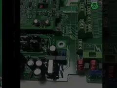
High density interconnect (HDI) PCBs represent one of the
fastest-growing segments of the PCB market. Because of its higher
circuitry density, the HDI technology can incorporate finer lines
and spaces, smaller vias and capture pads, and higher connection
pad densities. A high-density PCB features blind and buried vias
and often contains microvias that are .006 in diameter or even
less.
Key HDI PCB Benefits
The evolution of PCB HDI technology has given engineers greater
design freedom and flexibility than ever before. Designers using
HDI high density interconnect methods now can place more components
on both sides of the raw PCB if desired. In essence, an HDI PCB
gives designers more space to work with, while allowing them to
place smaller components even closer together. This means that a
high-density interconnect PCB ultimately results in faster signal
transmission along with enhanced signal quality.
HDI PCB is widely used to reduce the weight and overall dimensions
of products, as well as to enhance the electrical performance of
the device. The high-density PCB is regularly found in mobile
phones, touch-screen devices, laptop computers, digital cameras and
4G network communications. The HDI PCB is also prominently featured
in medical devices, as well as various electronic aircraft parts
and components. The possibilities for high-density interconnect PCB
technology seem almost limitless.
HDI PCB Applications
HDI boards are appropriate for a wide range of industries. As
mentioned above, you'll find them in all types of digital devices,
like smartphones and tablets, where miniaturization is key to the
effective application of the product. You can also find
high-density interconnect PCBs in automobiles, aircraft and other
vehicles that rely on electronics.
One of the most critical areas where the high-density PCB is making
huge inroads is in the medical arena. Medical devices frequently
need small packages with high transmission rates that only HDI PCBs
can supply. For example, an implant needs to be small enough to fit
in the human body, but any electronics involved in that implant
absolutely must efficiently allow for high-speed signal
transmission. Here, the HDI PCB indeed is a godsend. HDI PCBs can
also be useful in other medical equipment, like emergency room
monitors, CT scans and much more.
No matter your industry, you're probably already getting some ideas
about how high-density interconnect PCBs can make the electronics
you produce or use even better - get in touch with us PCBCart to
discuss it. We'll let you know if you're on the right track and
help you decide exactly how beneficial an HDI PCB can be to your
industry. Then, you can determine whether or not to take the next
step.
High Density PCBs of Impeccable Quality
Over the course of a decade in business, GLOBAL WELL Electronic has
established a hard-earned reputation for manufacturing PCBs of the
highest quality. Our custom PCB manufacturing capabilities enable
you to get the finest quality HDI PCBs at competitive prices
without min order quantity requirement. Our team run design for
manufacture check on your custom PCB file and consult with you to
ensure it is ready for manufacturing and that your boards will meet
your performance requirements. We also have an on-site quality
control department to verify the finished product meet your high
quality standards.
Our Services
1. PCB fabrication.
2. Turnkey PCBA: PCB+components sourcing+SMD and through-hole assembly
3. PCB clone, PCB reverse engineering.
PCB or PCBA Files Requests:
1. Gerber files of the bare PCB board
2. BOM (Bill of material) for assembly (please kindly advise us if
there is any acceptablecomponents substitution.)
3. Testing Guide & Test Fixtures if necessary
4. Programming files & Programming tool if necessary
5. Schematic if necessary
Global Well Electronic Inc. is a professional PCB solution supplier from Shenzhen, China, integrating PCB circuit board production and processing, STM processing and mounting, PCBA OEM, component purchasing, PCB/PCBA custom design-production- A comprehensive PCB circuit board company with one-stop turnkey service of processing-assembly-finished products. The company has a strong supply chain system, a professional and efficient collaborative team, a sound and complete quality control system, and the business philosophy of honesty and trustworthiness, customer first, and presents the products to everyone with low prices, reliable quality, high-quality service and after-sales service. client.
We provide total PCB solutions from PCB design to final mass production, including PCB fabrication and assembly, component sourcing, solder paste stencils, conformal coatings, and more. Serving the global electronics field, including industrial control, medical electronics, military equipment, power communication, automotive electronics, AI artificial intelligence, smart home and other industries.
Our factory located in Shenzhen, and have almost 300 employees, more than 30 production lines include SMT, DIP, automatic welding, aging test and assembly. We have SMT machines from Japan and Korea, automatic solder paste printing machines, solder paste inspection machine(SPI)12 temperature zone reflow soldering machine, AOI detector, X-RAY detector, wave soldering machine, EM PCB ,dispenser,laser print machine etc., Different line configurations can meet requirements from small sample order to bulk shipment.
Our company has obtained ISO 9001 quality system certification and ISO 14001 system certification. With multi-testingprocedures, our products carry out the quality system standard strictly.
| Order Quantity | 1-300,000,30000 Square Meter/Square Meters per Month module electronic board |
| Layer | 1,2,4,6,upto 40 layer |
| Material | FR-4,glass epoxy,FR4 High Tg,Rohs compliant,Aluminum,Rogers,etc |
| PCB type | Rigid,flexible,rigid-flexible |
| Shape | Any shape: Rectangular,round,slots,cutouts,complex,irregular |
| Max PCB dimensions | 20inch*20inch or 500mm*500mm |
| Thickness | 0.2~4.0mm, Flex 0.01~0.25'' |
| Thickness tolerance | ± 10% |
| Copper thickness | 0.5-4 oz |
| Copper thickness tolerance | ± 0.25oz |
| Surface finish | HASL,Nickle,Imm Gold,Imm Tin,Imm Silver,OSP etc |
| Solder mask | Green, red,white,yellow,blue,black, Double-sided |
| Silk screen | White,yellow,black,or negative, Double-sided or single-sided |
| Silk screen min line width | 0.006'' or 0.15mm |
| Min drill hole diameter | 0.01'',0.25mm.or 10 mil |
| Min trace/gap | 0.075mm or 3mil |
| PCB cutting | Shear,V-score,tab-routed |
| Turnkey PCBA | PCB+components sourcing+assembly+package |
| Assembly details | SMT and Thru-hole, ISO lines |
| Lead Time | Prototype: 15 work days. Mass order: 20~25 work days |
| Testing on products | Flying Probe Test, X-ray Inspection, AOI Test, functional test |
| Quantity | Min quantity: 1pcs. Prototype, small order, mass order, all OK |
| Files we need | PCB: Gerber files(CAM, PCB, PCBDOC) |
| Components: Bill of Materials(BOM list) | |
| Assembly: Pick-N-Place file | |
| PCB panel Size | Min size: 0.25*0.25 inches(6*6mm) |
| Max size: 20*20 inches(500*500mm) | |
| PCB Solder Type | Water Soluble Solder Paste, RoHS lead free |
| Components details | Passive Down to 0201 size |
| BGA and VFBGA | |
| Leadless Chip Carriers/CSP | |
| Double-sided SMT Assembly | |
| Fine Pitch to 0.8mils | |
| BGA Repair and Reball | |
| Part Removal and Replacement | |
| Component package | Cut Tape,Tube,Reels,Loose Parts |
| PCBA process | Drilling-----Exposure-----Plating-----Etaching Stripping-----Punching-----Electrical Testing-----SMT-----Wave Soldering-----Assembling-----ICT-----Function Testing-----Temperature - Humidity Testing |
Packing details:
PCBA are packed into plastic bags. Plastic bags are put into small carton. 4 small carton into a big carton.
A big carton: 35×32×40 cm size.
Shipping Express:
FedEx, DHL, UPS, TNT, EMS, private lines, etc.
Air freight, Sea shipping
If you need help on PCB layout, you can contact us and send the board to us. We also provide Reverse Engineering Service.
We have been providing PCB Manufacture for many years in China,and we have rich experience in product production and product assembly.We believe our team will provide high quality and low cost service for you.
Thank you very much for all your support .
Best Regareds.
Q1: Do you have a price list?
A: We are OEM Manufacturer. We produce products per Customer’s
designs and instructions. Hence we don’t have a price list.
Q2: What’s your MOQ for PCB, PCBA?
A: No MOQ for PCB and PCBA. We can do prototype and mass production
as well.
Q3: Are my files safe?
A: We can sign an NDA(Non-disclosure agreement).Your files are held
in complete safety and security.We protect the intellectual
property for our customers in the whole process.All documents from
customers are never shared with any third parties.
Q4: What is needed for PCB & PCBA quotation?
A: PCB: Quantity,Gerber file and technic requirements( board
material, board size, surface finish treatment, copper thickness,
board thickness).PCBA: PCB information,BOM,Testing documents.
Q5: What file formats do you accept for PCB and assembly?
A: Gerber file: CAM350 RS274X
PCB file: Protel 99SE,P-CAD 2001 PCB
BOM: Excel (PDF,word,txt)
Q6: Can you procure all parts in BOM for us?
A: YES, we can source all parts as per your bom list required.
Q7: Do you have after-sales product servicing available for your
customers?
A: Yes, for any quality problems, we will take our responsibility
to solve it for you at any time.