Add to Cart
|
|---|
Global Well as a professional PCB&PCBA manufacturer vendor, focuses on the production and manufacture of precision multilayer boards and special boards and has set up branches in many cities. The company adheres to the core values of "Customer First, Quality First, Continuous Innovation, Win-Win Cooperation", and is committed to providing global customers with good price, good quality, good service and fast delivery, creating greater value for customers and employees.
The company focuses on electronic products from PCB design- PCB production-SMT&DIP assembly - PCBA burn process and testing- Conformal coating - Electronic components procurement - finished product assembly and other one-stop manufacturing services. We are certified by U L, ISO9001,ISO13485, IATF1694, ISO14001, REACH, RoHS.
1. PCB fabrication.
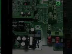
2. Turnkey PCBA: PCB+components sourcing+SMD and through-hole assembly
3. PCB clone, PCB reverse engineering.
PCB or PCBA Files Requests:
1. Gerber files of the bare PCB board
2. BOM (Bill of material) for assembly (please kindly advise us if
there is any acceptablecomponents substitution.)
3. Testing Guide & Test Fixtures if necessary
4. Programming files & Programming tool if necessary
5. Schematic if necessary
| Order Quantity | 1-300,000,30000 Square Meter/Square Meters per Month module electronic board |
| Layer | 1,2,4,6,upto 40 layer |
| Material | FR-4,glass epoxy,FR4 High Tg,Rohs compliant,Aluminum,Rogers,etc |
| PCB type | Rigid,flexible,rigid-flexible |
| Shape | Any shape: Rectangular,round,slots,cutouts,complex,irregular |
| Max PCB dimensions | 20inch*20inch or 500mm*500mm |
| Thickness | 0.2~4.0mm, Flex 0.01~0.25'' |
| Thickness tolerance | ± 10% |
| Copper thickness | 0.5-4 oz |
| Copper thickness tolerance | ± 0.25oz |
| Surface finish | HASL,Nickle,Imm Gold,Imm Tin,Imm Silver,OSP etc |
| Solder mask | Green, red,white,yellow,blue,black, Double-sided |
| Silk screen | White,yellow,black,or negative, Double-sided or single-sided |
| Silk screen min line width | 0.006'' or 0.15mm |
| Min drill hole diameter | 0.01'',0.25mm.or 10 mil |
| Min trace/gap | 0.075mm or 3mil |
| PCB cutting | Shear,V-score,tab-routed |
| Turnkey PCBA | PCB+components sourcing+assembly+package |
| Assembly details | SMT and Thru-hole, ISO lines |
| Lead Time | Prototype: 15 work days. Mass order: 20~25 work days |
| Testing on products | Flying Probe Test, X-ray Inspection, AOI Test, functional test |
| Quantity | Min quantity: 1pcs. Prototype, small order, mass order, all OK |
| Files we need | PCB: Gerber files(CAM, PCB, PCBDOC) |
| Components: Bill of Materials(BOM list) | |
| Assembly: Pick-N-Place file | |
| PCB panel Size | Min size: 0.25*0.25 inches(6*6mm) |
| Max size: 20*20 inches(500*500mm) | |
| PCB Solder Type | Water Soluble Solder Paste, RoHS lead free |
| Components details | Passive Down to 0201 size |
| BGA and VFBGA | |
| Leadless Chip Carriers/CSP | |
| Double-sided SMT Assembly | |
| Fine Pitch to 0.8mils | |
| BGA Repair and Reball | |
| Part Removal and Replacement | |
| Component package | Cut Tape,Tube,Reels,Loose Parts |
| PCBA process | Drilling-----Exposure-----Plating-----Etaching Stripping-----Punching-----Electrical Testing-----SMT-----Wave Soldering-----Assembling-----ICT-----Function Testing-----Temperature - Humidity Testing |
Packing details:
PCBA are packed into plastic bags. Plastic bags are put into small carton. 4 small carton into a big carton.
A big carton: 35×32×40 cm size.
Shipping Express:
FedEx, DHL, UPS, TNT, EMS, private lines, etc.
Air freight, Sea shipping
If you need help on PCB layout, you can contact us and send the board to us. We also provide Reverse Engineering Service.
We have been providing PCB Manufacture for many years in China,and we have rich experience in product production and product assembly.We believe our team will provide high quality and low cost service for you.
Thank you very much for all your support .
Best Regareds.