
Add to Cart
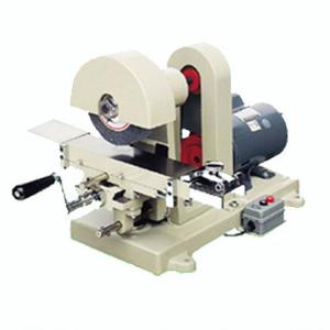
Laboratory Testing Machines Material Polished Tester HZ-1728 volume 50×60×40cm
Equipment description:
HZ-1728 Material Polished Tester polished, worn thin or grind the required thickness of the specimen.
Polished Surface Tester
The utility model belongs to a detection device, in particular to a
polished surface detector which can effectively detect tiny defects
and contamination on a wafer surface or a wafer subsurface.
With the rapid development of microelectronics technology, the
number of transistors integrated on semiconductor wafers is
increasing. Scientists from Fairchild Semiconductor Corporation in
the United States proposed decades ago that the number of
transistors that can be fabricated on a certain area of wafers
The number will double every eighteen months. In the past two
decades, the progress of integration has followed this law, and
scientists predict that this law will still exist in the next ten
to twenty years. Therefore, the area occupied by each transistor on
the wafer becomes smaller and smaller. It is predicted that in the
near future, each transistor will be composed of only a dozen or
even fewer crystal atoms. This development trend has put forward
stricter requirements for the development and production of
semiconductor wafers. Small defects or contamination will seriously
affect the performance of the device and even cause the device to
fail. For the development and production of large-scale and
ultra-large-scale integrated circuits, the first step is to reject
wafers with small defects or contamination, otherwise the yield
will be seriously affected. Therefore, the detection of
micro-defects and contamination on the surface or subsurface of the
mechanochemically polished wafer is gradually becoming one of the
key technologies related to the quality of the polished wafer of
semiconductor materials and the yield of the device manufacturing.
Unfortunately, there is currently no device that can effectively
detect microscopic defects and contamination on the wafer surface
or subsurface.
The purpose of this utility model is to provide a polishing surface
detector, which can accurately display the topography of the
surface and the subsurface of the polishing surface on a suitable
medium in the form of a visual image, and at the same time the
surface and subsurface inherent , due to processing and
environmental defects appear in the image. The materials it can
detect generally include metals, semiconductor materials and other
solid substances with similar properties.
As conceived above, the technical scheme of the present utility
model is: a polished surface detector, which is characterized in
that it is composed of a chassis, a control device, a light source
device placed in the chassis, a sample conveying device, an imaging
screen, and a camera device; wherein the sample conveying device is
composed of The device is connected with the sample conveying
control circuit; the imaging device is connected with the imaging
control circuit; the control circuit includes an amplification,
focal length, aperture control circuit and a translation stage
control circuit; the input ends of the above control circuits are
all connected with the output of the control device in the control
device End connection: The output end of the camera device is
connected to the input end of the monitor.
Technical parameters:
| Model | HZ-1728 |
| motor | 1/3HP |
| volume | 50×60×40cm |
| weight | 55kg |
| Power supply | 1∮,AC220V, 2.6A |