
Add to Cart
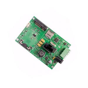
Electronic Component Sourcing Gold Finger Plating Thick Copper Boards
Electronic Component Sourcing Description:
1. A team of experts with more than 10 years of experience.
2. Professional component certified engineers and experienced
supply chain management team.
3. Pay attention to the latest international market information and
provide competitive prices.
4. Certified suppliers and parts.
PCB Manufacturing Parameters:
| Item | Technical Parameter |
| Layer | 2-64 |
| Thickness | 0.3-6.5mm |
| Copper Thickness | 0.3-12 oz |
| Min Mechanical Hole | 0.1mm |
| Min Laser Hole | 0.075mm |
| HDI | 1+n+1,2+n+2,3+n+3 |
| Max Aspect Ratio | 20:01 |
| Max Board Size | 650mm*1130mm |
| Min Width/Space | 2.4/2.4mil |
| Min Outline Tolerance | ±0.1mm |
| Impedance Tolerance | ±5% |
| Min PP Thickness | 0.06mm |
| Bow &Twist | ≤0.5% |
| Materials | FR4, High-Tg FR4, Rogers, Nelco, RCC, PTFE, M4, M6, TU862, TU872 |
| Surface Finished | HASL, HASL Pb Free Immersion Gold/Tin/Silver Osp, Immersion Gold+OSP |
| Special Capability | Gold Finger Plating, Peelable, Carbon ink |
Electronic Component Sourcing Introduction:
1. High density possible
Over the years, the high density of printed boards has been able to
develop correspondingly with the improvement of integrated circuit
integration and the advancement of mounting technology.
2. High reliability
Through a series of technical means such as inspection, testing,
and aging tests, the PCB can be guaranteed to work reliably for a
long time (usually 20 years).
3. designability
Requirements for various properties of PCB (electrical, physical,
chemical, mechanical, etc.) can be achieved through design
standardization, normalization, etc. In this way, the design time
is short and the efficiency is high.
4. producibility
PCB adopts modern management, which can realize standardization,
scale (quantization), and automatic production, so as to ensure the
consistency of product quality.
5. Testability
A relatively complete test method and test standard have been
established, and the qualification and service life of PCB products
can be detected and identified through various test equipment and
instruments.