Add to Cart
Empowering Innovation Discover Excellence at Our Advanced PCB Factory
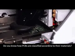
PCB Manufacturing Introduction:
Embark on a transformative journey of innovation at our cutting-edge PCB factory. We're not just a manufacturer; we're your partners in pushing the boundaries of electronics. Our extensive range of insulation materials, versatile layer options, and meticulous finishes lay the foundation for your most ambitious designs. Whether you require robust copper foil solutions, intricate multi-layer configurations, or specialized processes for high-frequency applications, we stand ready to meet your demands. With a commitment to exceptional materials, advanced technology, and stringent quality standards, our factory ensures that your vision becomes the reality of remarkable functionality and durability. Join us in revolutionizing electronics – where possibilities know no bounds.
PCB Manufacturing Parameters:
| Item | Technical Parameter |
| Layer | 2-64 |
| Thickness | 0.3-6.5mm |
| Copper Thickness | 0.3-12 oz |
| Min Mechanical Hole | 0.1mm |
| Min Laser Hole | 0.075mm |
| HDI | 1+n+1,2+n+2,3+n+3 |
| Max Aspect Ratio | 20:01 |
| Max Board Size | 650mm*1130mm |
| Min Width/Space | 2.4/2.4mil |
| Min Outline Tolerance | ±0.1mm |
| Impedance Tolerance | ±5% |
| Min PP Thickness | 0.06mm |
| Bow &Twist | ≤0.5% |
| Materials | FR4, High-Tg FR4, Rogers, Nelco, RCC, PTFE, M4, M6, TU862, TU872 |
| Surface Finished | HASL, HASL Pb Free Immersion Gold/Tin/Silver Osp, Immersion Gold+OSP |
| Special Capability | Gold Finger Plating, Peelable, Carbon ink |
PCB Manufacturing Process:
1. Gold-plating process: the vertical HASL process is very difficult to flatten very thin pads, which brings difficulty to SMT placement. In addition, the shelf life of the HASL is very short, and gold-plating just solves the problem. these problems.
2. Immersion gold process: The purpose of the immersion gold process is to deposit a nickel-gold coating with stable color, good brightness, flat coating and good solderability on the surface of the printed circuit board. Basically, it can be divided into four stages: pre-treatment (oil extraction, micro-etching, activation, post-immersion), nickel immersion, gold immersion, and post-treatment (waste gold washing, DI washing, drying)
3. Leaded HASL: Leaded eutectic temperature is lower than lead-free, the specific amount depends on the composition of the lead-free alloy, such as the total gold of SNAGCU 217 degrees, the soldering temperature is the eutectic immersion plus 30 degrees or 50 degrees, It depends on the actual adjustment, the lead eutectic is 183 degrees, the mechanical strength, brightness, etc. are better than lead-free.
4. Lead-free HASL: lead will increase the activity of tin wire in the soldering process, lead-tin wire is better than lead-free tin wire, but lead is poisonous, long-term use is not good for human health, and lead-free tin will It is brighter than lead-tin melting, so the solder joint is much stronger.
5. SOP (anti-oxidation): It has anti-oxidation, thermal shock resistance, and corrosion resistance. It is used to protect the copper surface from rusting (oxidation or carbonization) in a normal environment: but in the subsequent welding high temperature, this protection The film must be easily removed quickly by the flux so that the exposed clean copper surface can be melted and soldered immediately in a short time to become a firm solder joint.
PCB Manufacturing Advantages:
1. From PCB proofing to SMT placement, one-stop solution, reducing R&D costs and accelerating product launch.
2. Quick quotation and quick response.
3. The delivery date is fast, and the on-time delivery rate is over 95%
4. Excellent materials, advanced equipment, and strict quality system 5. Exclusive customer service one-to-one service, seamless connection throughout the process