Add to Cart
Elevate Your Electronics with Customized PCB Production Services
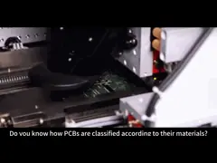
Innovative PCB Fabrication For Unsurpassed Quality And Flexibility
Key Steps In Printed Circuit Board Manufacturing:
1. Design: First, circuit board designers create circuit diagrams
and layouts using computer-aided design (CAD) tools. This includes
determining component locations, connections, and circuit paths.
2. Substrate Preparation: Non-conductive substrates are typically
made from fiberglass-reinforced epoxy resin. These substrates are
subsequently processed through cutting and lamination processes.
3. Conductive layer deposition: Deposition of conductive material
(usually copper) on the surface of a substrate to form a circuit
pattern. This can be done through chemistry, electroplating, or
other techniques.
Patterning: Using photolithography or etching to remove unwanted
portions of a conductive layer, leaving the desired circuit
pattern.
4. Component placement: Use automated equipment to accurately place
electronic components such as resistors, capacitors, and integrated
circuits onto circuit boards.
5. Soldering: Components and circuit boards are connected through a
soldering process. This can be done using surface-mount technology
(SMT) or through-mount technology (THT).
6. Testing and Quality Control: Once completed, the board goes
through a series of tests to ensure that all components are
connected correctly and the circuit is working properly. The
quality control process also includes visual inspection and
measurement.
Printed Circuit Board Fabrication Parameters:
Name | Printed Circuit Board Fabrication | Reinforcement type | PI, FR4, steel sheet, 3M glue, the electromagnetic shielding film |
Insulation | FR4 board, aluminum substrate, copper substrate, a ceramic substrate, PI (polycumimine), PET (poly) | Maximum size | 50OMM*1000MM |
Copper foil material | Glue-free calendered copper, rubber-rolled copper, glue-based electrolytic copper | Outer line width/line spacing | 0.065MM( 3MIL) |
number | 1-12 floors | Inner line width/line spacing | 0.065MM(3MIL) |
The finished board is thick | 0.07MM AND ABOVE (TOLERANCE +5%) | Minimum solder mask width | 0.10MM |
The inner layer is thick copper | 18-7OUM (1 ounce copper = 35UM) | Minimum mask bridge width | 0.05MM |
The outer layer is thick copper | 20-14OUM (1 plate copper = 35UM) | Minimum solder mask | 0.45MM |
Solder mask | Red oil, green oil, butter, blue oil, white oil, black oil, matte black oil, yellow film covered white film, black film | Minimum aperture | MECHANICAL DRILLING 0.2MM, LASER DRILLING 0,1MM |
word | Red, green, yellow, blue, white, black silver | Impedance Tolerance | 10% of soil |
Surface treatment | Anti-oxidation (OSP), tin spraying, gold immersion, gold plating, silver plating nickel plating, gold plating finger, carbon oil | Form tolerances | +0.05MM(LASER+0.005MM) |
Special processes | Thick copper plate, impedance plate, high-frequency plate, half-hole plate, orifice plate, hollow plate, single-layer copper foil, cross-sided gold finger plate, soft and hard combination | Molding method | V-cut, CNC, die punching, laser |
Printed Circuit Board Fabrication Factory Introduction:
Tongzhan Industrial Ltd. was established in 2011 in Shenzhen,
Guangdong Province. Tongzhan Industrial Ltd. is committed to
becoming a leading one-stop EMS supplier company, providing
customers with high-quality PCB series products. Tongzhan mainly
focuses on high-speed turnkey PCB layout design and PCB assembly
services, including PCB design, manufacturing, component
procurement, PCBA design and board making, supply chain services,
functional testing, conformal paint, complete assembly, etc. Our
corporate culture is to serve customers, customers always come
first. Customer-oriented, diligent and innovative, honest, happy,
transparent, customer-centric, professional, efficient, and
win-win. Our employees are passionate. Passion for Science. Passion
for technology.