Product Details
Pcb Manufacturer Waterproof Led Light PCB Board
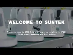
Suntek Contract Factory:
Suntek Group is a leading supplier in EMS field with one-stop
solution for PCB/FPC
assembly,Cable assembly,Mix technology assembly and Box-buildings.
Suntek Electronics Co., Ltd,as the major facility, located in Hunan
Prov,China;
BLSuntek Electronics Co., Ltd,as the new facility,located in Kandal
Prov,Cambodia.
Capabilities overview:
| Layers: | Rigid PCB 2 - 40 + Layers, Rigid-flex PCB 1 - 10Layers |
| Panel Size(max): | 21" x 24" |
| PCB Thickness: | 0.016" to 0.120" |
| Line & Spaces: | 0.003" / 0.003" Inner Layers; 0.004" Outer Layers |
| Hole Size: | 0.006" Thru Hole (Finished Size) and 0.004" Buried Via |
| Materials: | FR4, High Tg, Rogers, Halogen-free material, Teflon, Polyimide |
| Surface Finishes: | ENi/IAu, OSP, Lead-free HASL,Immersion Gold/Silver, Immersion Tin |
| Special Products: | Blind/ Buried Via(HDI 2+N+2), Rigid Flex |
Communication is the most important downstream application field of
PCB. PCB has a wide range of applications in various aspects such
as wireless network, transmission network, data communication and
fixed network broadband, and it is usually added value such as
backplane, high-frequency high-speed board, and multi-layer PCB board. Higher product. 5G is the next generation mobile communication
network, and there will be a large amount of infrastructure
construction demand by then, which is expected to greatly boost the
demand for communication boards.
Here are the most common applications of the telecommunication
industry that make efficient use of PCBs:
- Wireless communication systems
- Mobile phone tower systems
- Telephonic switching systems
- PBX systems
- Industrial wireless communication technology
- Technology for commercial phones
- Video conferencing technologies
- Communication technology used in space
- Cell transmission and tower electronics
- High speed servers and routers
- Electronic data storage devices
- Mobile communication systems
- Satellite systems and communication devices
- Video collaboration systems
- Land wired communication systems
- Technology for commercial phones
- Digital and analog broadcasting systems
- Voice over Internet Protocol (VoIP)
- Signal boost systems (online)
- Security technology and information communication systems
PCB Requirements
Communication devices require PCBs to provide robust and reliable
connectivity solutions for complex high speed components. Signal
integrity needs to be maintained as signals travel between
transceivers, antennas, power amplifiers and more. These
requirements generally include:
- High-Frequency Performance
Many communication device signals operate at high frequencies in
the microwave band. For example, smartphones incorporate multiband
antennas that support 4G and 5G frequency bands – 700 MHz to 5 GHz
for the latest generation. This requires PCB materials and construction to enable proper signal transmission without
degradation through dielectric power loss or leaky RF conduction
paths. We carefully select substrates and lamination materials
tailored for high frequency operation based on dielectric constant,
loss tangent, thermal conductivity, TCE and other parameters. - High Speed Signal Handling
In addition to frequency, data rate throughput capacity is equally
important. Cutting-edge phones with multi-Gbps Wi-Fi 6 speeds, high
bandwidth wireless interfaces need PCBs with fine line traces and
spaces (4-6 mil line/space is common for data lines). Short signal
paths routed close together require low loss, tight impedance
tolerance laminates as well as careful stackups for characteristic
impedance control. And a robust power distribution network is key
for clean power delivery to signal ICs and FPGAs operating at high
clock rates. We design layer counts, trace dimensions, dielectrics
and laminate materials specifically to maintain signal integrity in
high speed signal paths. - EMI and Crosstalk Prevention
With complex components in close proximity and interacting at high
frequencies, communication PCBs must prevent unwanted coupling
between traces. Short signal return paths, reference planes and
proper component placement facilitate field confinement. Our
engineers utilize careful stackup symmetry, selective
isolation/shielding around sensitive components, ground stitching
vias alongside traces, and special treatments to eliminate EMI
emission and minimize crosstalk in dense layouts with high speed
traces throughout multilayer boards.
Quality and Reliability
Delivering the highest reliability PCB solutions for
mission-critical communication systems demands strict process and
quality management upholding industry standards. As an ISO 9001
certified manufacturer, we’ve implemented robust infrastructure
spanning materials qualification to volume fabrication monitoring:
- IPC Standards
We benchmark quality against IPC J-STD-001, IPC-A-600 and other
widely adopted PCB quality specifications. Audits of our facilities
verify standard classes conformance through acceptance testing of
fabricated boards as well as process reviews targeting continual
improvement per IPC guidelines. IPC certifications validate
disciplined, optimized fabrication workflows. - Advanced Quality Planning
Reliability risks are systematically identified during NPI through
process controls selection, PFMEA/DRBFM and test vehicle
measurements establishing performance baselines. We tailor process
qualification, verification testing and QA sampling plans per
customer requirements and design risk assessments. Each producible
design has associated quality plan generating 1st pass yields. - Traceability
Raw materials receipt to finished boards shipped are tracked by ERP
software tools with batch/lot traceability. Barcode work orders
follow boards through process documenting each fabrication,
inspection and test operation in our secured database. Complete
traceability with records retention delivers the transparency
customers expect from their trusted PCB producers.
Company Profile
Suntek Group is a professional contract factory on one-stop
solution for PCB/FPC assembly,Cable assembly,Mix technoloty
assembly and Box-build assembly.
Suntek Electronics Co.,Ltd,as a major facility,located in Hunan province,China;
BLSuntek Electronics Co.,Ltd,as the new facility,located in Kandal province,Cambodia.

With ISO9001:2015,ISO13485:2016,IATF 16949:2016 and UL E476377
certified.We deliver qualified products with competitive price to clients all
over the world.We have the advanced manufacturing equipments,proficient
technology,professional engineer team,purchasing team,quality team
and management team to guarantee the high quality products and on
time delivery.
Our products are widely used in industrial
control,auto,telecommunications,medical equipment,consumer
electronics and etc.
core is "Quality wins Market, Ideas create the Future".
The Applications of the products we manufacture:
The glimps of Suntek China
The glimps of BLSuntek Cambodia