
Add to Cart
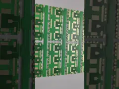
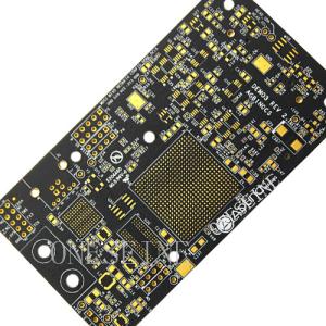
14 Layer PCB HDI Vias In Pad BGA Multilayer Pcb Construction
PCB introduction:
Layer | 14 | Color | Black |
Material | Fr4 | Min hole | 0.15 |
Surface | Gold plated | Special | Vias in pad |
Min line | 4mil | BGA | 2 |
14 Layer Fr4 Via-In-Pad PCB printed circuit board
Perhaps one of the greatest benefits of via fill is the option to implement Via In-Pad. This process is becoming more and more popular and preferred as opposed to using the traditional "dog bone" method to transfer signal from the BGA, through the via, and on to inner layers. In this process, also known as active pad, vias are filled, planarized, plated over with copper. While the Via-In-Pad process does increase cost there can be significant benefits over conventional through hole technology.
Some key benefits are:
Tighter BGA pitches
Increased thermal dissipation
Reduced layer count or board size, which ultimately may reduce cost
Improved routing density (higher density per layer)
Strengthening Pad attachment
Gives high frequency designs the shortest possible route to bypass capacitors
Overcomes high speed desogn issues and constraints such as low inductance
Via in pad technology gets you intermediate density at a slightly higher cost compared to blind/buried vias. The extra dollars go into added manufacturing steps and material cost. But the benefits you get are:
Fan out fine pitch (less than .75mm)
Meets closely packed placement requirements
Better thermal management
Overcomes high speed design issues and constraints i.e. low inductance
No via plugging is required at component locations
Provides a flat, co-planar surface for component attachment
What is prepreg in PCB?
Prepreg, which is an abbreviation for pre impregnated, is a fibre weave impregnated with a resin bonding agent. It is used to stick the core layers together. The core layers being FR4 with copper traces. The layer stack is pressed together at temperature to the required board finish thickness.
14 Layer pcb stack up
What is layer stackup?
The PCB stackup is the substrate upon which all design components are assembled. A poorly designed PCB stackup with inappropriately selected materials can degrade the electrical performance of signal transmission, power delivery, manufacturability, and long term reliability of the finished product.
How many layers can a PCB have?
It is usually even and includes the two outer layers. Most main boards have between 4 and 8 layers, but PCBs with almost 100 layers can be made
14 layer and 16 Layer also common orders here in Oneseine
Multilayer pcb stack up
The stack-up of a multilayer PCB refers to the arrangement and order of the layers in the PCB construction. The stack-up is a critical aspect of PCB design as it determines the electrical performance, signal integrity, impedance control, and thermal characteristics of the board. The specific stack-up configuration depends on the requirements of the application and the design constraints. Here is a general description of a typical multilayer PCB stack-up:
1,Signal Layers: The signal layers, also known as the routing layers, are where the copper traces that carry electrical signals are located. The number of signal layers depends on the complexity of the circuit and the desired density of the PCB. The signal layers are typically sandwiched between the power and ground planes for better signal integrity and noise reduction.
2,Power and Ground Planes: These layers provide a stable reference for the signals and help distribute power and ground throughout the PCB. The power planes carry the supply voltages, while the ground planes serve as return paths for the signals. Placing power and ground planes adjacent to each other reduces the loop area and minimizes electromagnetic interference (EMI) and noise.
3,Prepreg Layers: Prepreg layers consist of insulating material impregnated with resin. They provide insulation between adjacent signal layers and help bond the layers together. Prepreg layers are typically made of fiberglass-reinforced epoxy resin (FR-4) or other specialized materials.
4,Core Layer: The core layer is the central layer of the PCB stack-up and is made of a solid insulating material, often FR-4. It provides mechanical strength and stability to the PCB. The core layer may also include additional power and ground planes.
5,Surface Layers: The surface layers are the outermost layers of the PCB, and they can be signal layers, power/ground planes, or a combination of both. The surface layers provide connectivity to external components, connectors, and soldering pads.
6,Soldermask and Silkscreen Layers: The soldermask layer is applied over the surface layers to protect the copper traces from oxidation and prevent solder bridges during the soldering process. The silkscreen layer is used for component markings, reference designators, and other text or graphics to assist in PCB assembly and identification.
The exact number and arrangement of layers in a multilayer PCB stack-up vary depending on the design requirements. More complex designs may have additional power planes, ground planes, and signal layers. Additionally, controlled impedance traces and differential pairs may require specific layer arrangements to achieve desired electrical characteristics.
It's important to note that the stack-up configuration should be carefully designed, taking into consideration factors such as signal integrity, power distribution, thermal management, and manufacturability, to ensure the overall performance and reliability of the multilayer PCB.
There are several kinds of multilayer PCBs that are used in different applications. Here are some common types:
Standard Multilayer PCB: This is the most basic type of multilayer PCB, typically consisting of four to eight layers. It is widely used in general electronic devices and applications where moderate complexity and density are required.
High-Density Interconnect (HDI) PCB: HDI PCBs are designed to provide higher component density and finer traces than standard multilayer PCBs. They often have microvias, which are very small diameter vias that allow for more interconnections in a smaller space. HDI PCBs are commonly used in smartphones, tablets, and other compact electronic devices.
Flex and Rigid-Flex PCB: These types of multilayer PCBs combine flexible and rigid sections into a single board. Flex PCBs use flexible materials like polyimide, while rigid-flex PCBs incorporate both flexible and rigid sections. They are used in applications where the PCB needs to bend or conform to a specific shape, such as in wearable devices, medical equipment, and aerospace systems.
Sequential Lamination PCB: In sequential lamination PCBs, the layers are laminated together in separate groups, allowing for a higher number of layers. This technique is used when a large number of layers, such as 10 or more, are required for complex designs.
Metal Core PCB: Metal Core PCBs have a layer of metal, usually aluminum or copper, as the core layer. The metal core provides better heat dissipation, making them suitable for applications that generate a significant amount of heat, such as high-power LED lighting, automotive lighting, and power electronics.
RF/Microwave PCB: RF (Radio Frequency) and microwave PCBs are designed specifically for high-frequency applications. They use specialized materials and manufacturing techniques to minimize signal loss, impedance mismatch, and electromagnetic interference. RF/Microwave PCBs are commonly used in wireless communication systems, radar systems, and satellite communications.
Multilayer pcb application:
Multilayer PCBs find application across various industries and electronic devices where complex circuitry, high density, and reliability are required. Some common applications of multilayer PCBs include:
Consumer Electronics: Multilayer PCBs are extensively used in consumer electronic devices such as smartphones, tablets, laptops, gaming consoles, televisions, and audio systems. These devices require compact designs and high-density interconnections to accommodate numerous components.
Telecommunications: Multilayer PCBs play a crucial role in telecommunications equipment, including routers, switches, modems, base stations, and network infrastructure. They enable efficient signal routing and facilitate the high-speed data transmission required in modern communication systems.
Automotive Electronics: Modern vehicles incorporate a wide range of electronics for functions like engine control, infotainment systems, advanced driver-assistance systems (ADAS), and telematics. Multilayer PCBs are used to accommodate the complex circuitry and ensure reliable performance in automotive environments.
Industrial Equipment: Multilayer PCBs are utilized in industrial equipment such as control systems, robotics, automation systems, and manufacturing machinery. These PCBs provide the necessary interconnections for precise control and monitoring of industrial processes.
Aerospace and Defense: The aerospace and defense industries rely on multilayer PCBs for avionics systems, radar systems, communication equipment, guidance systems, and satellite technology. These applications demand high reliability, signal integrity, and resistance to harsh environments.
Medical Devices: Medical devices and equipment, including diagnostic tools, imaging systems, patient monitoring devices, and surgical instruments, often utilize multilayer PCBs. These PCBs enable the integration of complex electronics and assist in accurate and reliable medical diagnostics and treatments.
Power Electronics: Multilayer PCBs are employed in power electronics applications, such as inverters, converters, motor drives, and power supplies. They help manage high currents, heat dissipation, and efficient power distribution.
Industrial Control Systems: Multilayer PCBs are utilized in industrial control systems for process control, factory automation, and robotics. These systems require reliable and high-performance PCBs to ensure precise control and monitoring of industrial processes.