Add to Cart
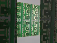
Double sided Metal Core Copper Base MC PCB printed circuit boards
Oneseine PCB information:
PCB material:metal core copper base
Layer:2
Copper weight:6OZ
Solder mask:Blue
Outline: Routing, punching, V-Cut
Soldermask: White/Black/Blue/Green/Red Oil
Legend/Silkscreen Color: Black/White
Surface finishing: Immersion Gold, HASL, OSP
Packing: Vacuum/Plastic bag
Samples L/T: 5~7 Days
MP L/T: 6~8 Days
Copper Core PCB
Copper core PCB is a copper substrate + Insulated layer + copper
circuits layer PCB,also, it is called copper substrate pcb, copper
based pcb,copper clad pcb.
As a MCPCB manufacturer,oneseine made various Copper core PCB for customers,
Which used for High Power LED lighter ( 1000W+ ) and power supply.
In LED field,there are 4 types of Copper based Circuit Board.
1. General Copper substrate Board.
2. COB Copper PCB(Chip on Board copper PCB)
LED chip Direct thermal sink to copper substrate.
3. Direct thermal path,no dielectric layer under the thermal path pad.
4.Direct thermal path,no dielectric layer,Aluminum-copper pcb.
Generally speaking, aluminum is the most economic option considering thermal conductivity, rigidness, and cost. Therefore, the base/core material of normal Metal Core PCB are made of aluminum. In Oneseine, if not special request, or notes, the metal core refer will be aluminum, then MCPCB will means Aluminum Core PCB. If you need Copper Core PCB, Steel Core PCB, or Stainless steel core PCB, you should add special notes in drawing.
Sometimes people will use abbreviation “MCPCB”, instead of the full name as Metal Core PCB, or Metal Core Printed Circuit Board. And also used different word refers the core/base, so you will also see different name of Metal Core PCB, such as Metal PCB, Metal Base PCB, Metal Backed PCB, Metal Clad PCB and Metal Core Board and so on.
MCPCBs are used instead of traditional FR4 or CEM3 PCBs because of the ability to efficiently dissipate heat away from the components. This is achieved by using a Thermally Conductive Dielectric Layer.
According to different location of metal core and trace layers of PCB, right now, we divide into five basic types:
Single Layer MCPCB(only one trace layer one one side);
COB MCPCB (chip-on-board MCPCB, one trace layers);
Double Layers MCPCB (two trace layers on the same side;
Double Sided MCPCB (two trace layers on each side);
Multi Layers MCPCB (More than 2 trace layers per board);
Kinds of metal core PCB:
Metal core pcb production:
Metal Core PCBs (Printed Circuit Boards) are specialized circuit boards that have a base layer made of metal, typically aluminum, instead of the traditional FR4 (fiberglass-reinforced epoxy) material. These boards are commonly used in applications that require efficient heat dissipation, such as high-power LED lighting, power supplies, automotive electronics, and power electronics.
The production process for metal core PCBs is similar to that of traditional PCBs but with some additional considerations for the metal layer. Here are the general steps involved in the production of metal core PCBs:
1,Design: Create a PCB layout using PCB design software, taking into account the circuit requirements, component placement, and thermal considerations.,
2,Material Selection: Choose the appropriate metal core material for your application. Aluminum is the most common choice due to its good thermal conductivity, lightweight, and cost-effectiveness. Other options include copper and alloys like aluminum-backed copper-clad laminates.
3,Base Layer Preparation: Start with a metal sheet of the chosen material, typically aluminum. The sheet is cleaned and treated to remove any contaminants and oxidation, ensuring good adhesion between the metal and the PCB layers.,
4,Lamination: Apply a layer of thermally conductive dielectric material, such as an epoxy-based resin, on both sides of the metal core. This dielectric layer provides electrical insulation and helps to bond the copper layers.
5,Copper Cladding: Add a thin layer of copper to both sides of the dielectric material using methods like electroless copper plating or a combination of electroless and electrolytic copper plating. The copper layer serves as the conductive traces and pads for the circuit.,
6,Imaging: Apply a photosensitive resist layer over the copper surfaces. Expose the resist layer to UV light through a photomask that contains the desired circuit pattern. Develop the resist to remove the unexposed areas, leaving the circuit pattern on the copper.
7,Etching: Submerge the board in an etchant solution that removes the unwanted copper, leaving only the circuit traces and pads as defined by the resist layer. Rinse and clean the board thoroughly after etching.,
8,Drilling: Drill holes through the board at designated locations for component mounting and interconnection. These holes are typically plated through with copper to provide electrical continuity between the layers.
9,Plating and Surface Finish: Further copper plating may be performed to increase the thickness of the circuit traces and pads if required. Apply a surface finish, such as HASL (Hot Air Solder Leveling), ENIG (Electroless Nickel Immersion Gold), or OSP (Organic Solderability Preservative), to protect the exposed copper and facilitate soldering.,
10,Solder Mask and Silkscreen: Apply a solder mask to cover the copper traces and pads, leaving only the desired soldering areas exposed. Apply a silkscreen layer to add component labels, reference designators, and other markings.
11,Testing and Inspection: Conduct electrical testing, such as continuity checks and netlist verification, to ensure the integrity of the circuit. Inspect the board for any manufacturing defects or errors.,
12,Assembly: Mount electronic components onto the metal core PCB using automated pick-and-place machines or manual soldering, depending on the complexity and volume of production.
13,Final Testing: Perform functional testing on the assembled PCB to verify its performance and ensure it meets the required specifications.
It's important to note that the production process can vary depending on the specific requirements of the metal core PCB, the chosen materials, and the manufacturer's capabilities. It's recommended to consult with a professional PCB manufacturer for specific guidelines and recommendations tailored to your project.
Metal core pcb thickness:
The thickness of a metal core PCB (Printed Circuit Board) refers to the overall thickness of the PCB, including the metal core and all the additional layers. The thickness of a metal core PCB is determined by several factors, including the application requirements, the choice of metal core material, and the number of copper layers and their thickness.
Typically, metal core PCBs have a total thickness ranging from 0.8mm to 3.2mm, although thicker boards can be produced for specific applications. The metal core itself contributes to a significant portion of the overall thickness.
The metal core thickness can vary depending on the thermal conductivity requirements and mechanical stability needed for the specific application. Aluminum is one of the commonly used metal core materials due to its good thermal conductivity and lightweight nature. The aluminum core thickness can range from around 0.5mm to 3.0mm, with 1.0mm and 1.6mm being common choices.
In addition to the metal core, the overall thickness of the PCB includes other layers such as dielectric material, copper traces, solder mask, and surface finish. The dielectric layer thickness is typically in the range of 0.05mm to 0.2mm, while the copper layer thickness can vary depending on the specific requirements of the circuit design, such as current-carrying capacity. Typical copper layer thicknesses range from 17µm (0.5oz) to 140µm (4oz) or higher.
It's important to note that the thickness requirements for metal core PCBs can vary significantly based on the application and specific design considerations. It's recommended to consult with a PCB manufacturer or design engineer to determine the appropriate thickness based on your project's requirements and constraints.