Add to Cart
Fast Pcbway Electronic Products Prototype SMT DIP PCB Assembly
General information:
Base material:FR4
Layer:2
Name:Amplifier PCB assembly
Surface finish:HASL lead free
Copper thickness:1OZ
Test: Flying probe test, X-ray Inspection,AOI (Automated Optical Inspection)
ICT (In-Circuit Test)/Functional Testing
PCB Assembly General Manufacturing Capabilities: | |
Type of Assembly | THD (Thru-Hole Device), SMT (Surface-Mount Technology), SMT & THD mixed, Double-sided SMT and THD assembly. |
Solder Type | Water Soluble Solder Paste, Leaded process and Lead-Free (RoHS) |
Components | Passives parts, smallest size 0201 BGA, uBGA, QFN, POP, and Leadless chips Fine Pitch to 0.8Mils; BGA Repair and Reball; Part Removal and Replacement Connectors and terminals |
Bare Board Size | Smallest:0.25’’x 0.25’’ (6.35mm x 6.35mm) Largest: 20’’ x 20’’ (508mm x 508mm) |
Min. IC Pitch | 0.012’’ (0.3mm) |
QFN Lead Pitch | 0.012’’ (0.3mm) |
Max. BGA size | 2.90’’ x 2.90’’ (74mm x 74mm) |
Type of Service | Turn-key, partial turn-key or consignment |
Testing | X-ray Inspection AOI (Automated Optical Inspection) ICT (In-Circuit Test)/Functional Testing |
Component packaging | Reels, cut tape, Tube and tray, Loose parts and bulk |
PCB Assembly Concept:
PCBA is the abbreviation of printed circuit board + Assembly, that is to say, the PCB bare board through the SMT, and then through the whole process of the DIP plug-in, referred to as the PCBA, which is commonly used in China, and the standard in Europe and America is PCB 'A, is added to the ramp point. This is called the official idiom, we communicate with foreign customers or when the promotion, they often ask what is PCBA.
A printed circuit board (PCB) mechanically supports and electrically connects electronic components using conductive tracks, pads and other features etched from copper sheets laminated onto a non-conductive substrate. Components – capacitors, resistors or active devices – are generally soldered on the PCB. Advanced PCBs may contain components embedded in the substrate.
PCBs can be single sided (one copper layer), double sided (two copper layers) or multi-layer (outer and inner layers). Conductors on different layers are connected with vias. Multi-layer PCBs allow for much higher component density.
FR-4 glass epoxy is the primary insulating substrate. A basic building block of the PCB is an FR-4 panel with a thin layer of copper foil laminated to one or both sides. In multi-layer boards multiple layers of material are laminated together.
Printed circuit boards are used in all but the simplest electronic products. Alternatives to PCBs include wire wrap and point-to-point construction. PCBs require the additional design effort to lay out the circuit, but manufacturing and assembly can be automated. Manufacturing circuits with PCBs is cheaper and faster than with other wiring methods as components are mounted and wired with one single part.
A minimal PCB with a single component used for easier modeling is called breakout board.
PCB/PCBA Order tips: |
A. PCB order: Please provide Gerber File and manufacturing specifications. B. PCBA order: Please provide Gerber File, Manufacturing specification, BOM list and Pick & Place/XY file. C. Reverse engineering and PCB copy service can be supplied with your PCB sample. D. PCB design need detail information about the function or supply the drawing. E. Any further questions, welcome to contact us by sending email. |
.
Main PCBA Equipments
ITEM | Device Name | Model | Brand Name | Qty | Remarks |
1 | Full Automatic Screen Printer | DSP-1008 | DESEN | 8 | |
2 | SMT Machine | YG200 | YAMAHA | 5 | 8 SMT Line |
3 | SMT Machine | YV100XG | YAMAHA | 3 | |
4 | SMT Machine | YG100XGP | YAMAHA | 19 | |
5 | SMT Machine | YV88 | YAMAHA | 5 | |
6 | Reflow Soldering | 8820SM | NOUSSTAR | 4 | |
7 | Reflow Soldering | XPM820 | Vitronics Soltec | 3 | |
8 | Reflow Soldering | NS-800 II | JT | 1 | |
9 | Solder Paste Inspection | REAL-Z5000 | REAL | 1 | |
10 | Automatic Optical Inspection System | B486 | VCTA | 3 | |
11 | Automatic Optical Inspection System | HV-736 | HEXI | 5 | |
12 | X-Ray | AX8200 | UNICOMP | 1 | |
13 | BGA Re-work | MS8000-S | MSC | 1 | |
14 | Universal 4*48-pindrive concurrent multiprogramming system | Beehive204 | ELNEC | 3 | |
15 | Automatic Plug-In machines | XG-3000 | SCIENCGO | 2 | |
16 | Automatic wave soldering system | WS-450 | JT | 1 | 3 DIP LINE |
17 | Automatic wave soldering system | MS-450 | JT | 2 |
The PCB assembly process typically includes the following steps:
Component Procurement: The required electronic components are sourced from suppliers. This involves selecting components based on specifications, availability, and cost.
PCB Fabrication: The bare PCBs are manufactured using specialized techniques such as etching or printing. The PCBs are designed with copper traces and pads to establish electrical connections between the components.
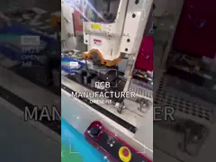
Component Placement: Automated machines, called pick-and-place machines, are used to accurately place surface mount components (SMD components) on the PCB. These machines can handle a large number of components with precision and speed.
Soldering: Once the components are placed on the PCB, soldering is performed to establish electrical and mechanical connections. There are two common methods used for soldering: a. Reflow Soldering: This method involves applying solder paste to the PCB, which contains small solder balls. The PCB is then heated in a reflow oven, causing the solder to melt and create connections between the components and the PCB. b. Wave Soldering: This method is typically used for through-hole components. The PCB is passed over a wave of molten solder, which creates solder connections on the bottom side of the board.
Inspection and Testing: After soldering, the assembled PCBs undergo inspection to check for defects, such as solder bridges or missing components. Automated optical inspection (AOI) machines or human inspectors perform this step. Functional testing may also be conducted to ensure the PCB operates as intended.
Final Assembly: Once the PCBs pass inspection and testing, they can be integrated into the final product. This may involve additional assembly steps, such as attaching connectors, cables, enclosures, or other mechanical components.
Certainly! Here are some additional details about PCB assembly:
Surface Mount Technology (SMT): Surface mount components, also known as SMD (Surface Mount Device) components, are widely used in modern PCB assembly. These components have small footprints and are mounted directly onto the surface of the PCB. This allows for higher component density and smaller PCB sizes. SMT components are typically placed using automated pick-and-place machines, which can handle components of various sizes and shapes.
Through-Hole Technology (THT): Through-hole components have leads that pass through holes in the PCB and are soldered on the opposite side. While SMT components dominate modern PCB assembly, through-hole components are still used for certain applications, especially when components require extra mechanical strength or high power handling capabilities. Wave soldering is commonly used for soldering through-hole components.
Mixed Technology Assembly: Many PCBs incorporate a combination of surface mount and through-hole components, referred to as mixed technology assembly. This allows for a balance between component density and mechanical strength, as well as accommodating components that are not available in surface mount packages.
Prototype vs. Mass Production: PCB assembly can be performed for both prototype and mass production runs. In prototype assembly, the focus is on building a small number of boards for testing and validation purposes. This may involve manual component placement and soldering techniques. Mass production, on the other hand, requires high-speed automated assembly processes to achieve efficient and cost-effective production of large quantities of PCBs.
Design for Manufacturing (DFM): DFM principles are applied during the PCB design phase to optimize the assembly process. Design considerations such as component placement, orientation, and proper clearances help ensure efficient assembly, reduce manufacturing defects, and minimize production costs.
Quality Control: Quality control is an integral part of PCB assembly. Various inspection techniques are employed, including visual inspection, automated optical inspection (AOI), and X-ray inspection, to detect defects such as solder bridges, missing components, or incorrect orientations. Functional testing may also be conducted to verify the proper operation of the assembled PCB.
RoHS Compliance: Restriction of Hazardous Substances (RoHS) directives restrict the use of certain hazardous materials, such as lead, in electronic products. PCB assembly processes have adapted to comply with RoHS regulations, using lead-free soldering techniques and components.
Outsourcing: PCB assembly can be outsourced to specialized contract manufacturers (CMs) or electronic manufacturing service (EMS) providers. Outsourcing allows companies to leverage the expertise and infrastructure of dedicated assembly facilities, which can help reduce costs, increase production capacity, and access specialized equipment or expertise.