Lightweight design, Protect Wafer Safe Transport, Clean PP Material
The vertical wafer box is designed specifically for the
semiconductor industry, aiming to provide efficient wafer storage
and transportation solutions. Its unique vertical structure and
superior protective performance make it an important tool for
improving production efficiency and ensuring product safety.
Ideal for transferring wafers between processes, this box is not
suitable for use in chemical processes. Its compact design also
helps to reduce transportation costs.
Save Space: The vertical design occupies less ground space, making it easier
to store more wafers in a limited workspace.
Better Visibility: The vertical structure makes the arrangement of wafers clearer,
making it easier for operators to quickly inspect and access them.
Strong Compatibility: Adapt to multiple devices and production lines, with high
flexibility and easy integration into existing processes.
Packing and Shipping:
Packaging:
The Wafer Storage Box is first wrapped in protective bubble wrap to
prevent any damage during transit.
Next, the box is placed in a sturdy cardboard box to provide
additional protection.
To ensure the box stays secure, it is sealed with high-quality
packing tape.
A label is then attached to the box with the product name,
quantity, and any other necessary information.
Shipping:
For international orders, we carefully package the box and ship it
via air or sea freight to ensure timely and safe delivery.
We provide tracking information for all orders so you can easily
monitor the status of your shipment.
If any issues arise during shipping, our customer service team is
available to assist you and resolve the problem.
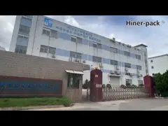
Company Profile
Hiner-pack has leading mold processing and injection molding
equipment, high-grade dust-free cleaning line and a variety of
testing equipment.Meanwhile,Hiner-pack has established a depth of
cooperation with well-known enterprises and built a polymer
material R&D base with domestic well-known universities as well
as scientific research institutions.
Hiner-pack has mastered special processing technique and
manufacturing in semiconductor packaging raw material field.Owned a
lot of inventions and practical new patents.Through years of
unremitting efforts,Hiner-pack has a professional R&D team to
improve semiconductor packaging products, new products continue to
launch,and to solve the customer demand for high quality products.
Learn more about our company through our official website https://www.hiner-pack.com/english/
Learn more JEDEC TRAY IC TRAY information through our official
websitehttps://www.jedecictrays.com/