Wafer Package System: Our Wafer Package System offers a secure and efficient way to
transfer wafers. With years of experience and proven technology,
this system can handle even the most fragile of wafers, including
thin wafers for TSV chips and compound wafers.
Conductive and Shock-Resistant Wafer Carrier:The wafer carrier is designed to protect wafers from potential
risks during transportation. It is conductive, clean, and
shock-resistant, offering protection against die bond corrosion,
electrostatic discharge (ESD), and physical damage.
Efficient and Compact Design:The compact and stackable design of our wafer carrier ensures
efficient wafer shipping. It can accommodate 1 to 25 wafers, making
it perfect for any size shipment.
Superior Wafer Protection: Our wafer carrier is made from low ionic and low outgassing wafer
Grade PP material, providing superior protection for your wafers.
It also has compounded ESD properties, further ensuring maximum
protection for your wafers and devices.
Features:
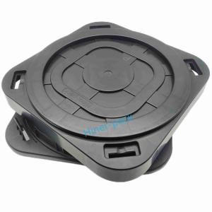
Product Name: Wafer Carrier Box
Capacity: 25PCS
Cleanliness*1: Clean Room Use(Cleaning And Packing)
Incoterms: EXW,FOB,CIF,DDU,DDP
Size: Standard For Wafer Size 300mm
Cleanliness*2: Ordinary Environment
Conductive PP Material
Certification: This Wafer Carrier Box has been certified by ROHS LPC IC Report,
ensuring its compliance with international standards for safety and
quality.
Packaging Details: The Wafer Carrier Box is double packed after cleaning to ensure
maximum protection during transportation and storage.
Supply Ability: With a production capacity of 300 to 500 sets per day, Hiner-pack
can meet the demands of small to large-scale customers.
Material: This product is made of conductive PP (Polypropylene), a
high-quality material known for its strength and conductivity.
Cleanliness: The Wafer Carrier Box is suitable for clean room use, as it
undergoes thorough cleaning and packing processes before being
shipped to customers.
Technical Parameters:
Name
Horizontal Wafer Shipper
Design
Ergonomic Open/Close Design
OEM/ODM
Accept Customization
Advantage
Optimized Wafer Shipment
Set Contains
Base, Lid
Material
Conductive PP
Applications:
The Wafer Carrier Box is specifically designed for the
transportation and storage of wafers in the semiconductor industry.
It is commonly used in wafer fabrication plants, testing
facilities, and research laboratories. This product provides a safe
and secure way to transport and store wafers, protecting them from
potential damage and contamination.
The Wafer Carrier Box, also known as Horizontal Wafer Shipper, is a
high-quality and reliable product manufactured by Hiner-pack in
China. With its sturdy and durable design, it provides a safe and
secure way to transport and store wafers in the semiconductor
industry. This product is suitable for clean room use, promotes
cleanliness, and is versatile for various wafer sizes. It has been
certified by ROHS LPC IC Report, ensuring its compliance with
international standards. With a production capacity of 300 to 500
sets per day, Hiner-pack can meet the demands of small to
large-scale customers. Choose the Wafer Carrier Box for your wafer
shipping and storage needs and experience its superior quality and
reliability.
Advantage:
Base Lid And Cassette options to meet your specific needs
Packing and protection for silicon wafers during transit
Customization of Hiner-pack brand name and logo on the carrier box
Model number HWS-Horizontal Wafer Shippers available in size range
of 300mm
Made in China with ROHS LPC IC Report certification
Flexible minimum order quantity with negotiable prices
Unit prices that vary according to delivery methods and quantities
Double pack after thorough cleaning for maximum hygiene and safety
Fast delivery within 2~3 weeks
TT 100% prepayment as payment terms
High supply ability of 300~500 sets per day
Standard size for wafer size range of 300mm
Sleek and professional black color
Superior wafer protection with our carrier box
Company Profile
Hiner-pack has leading mold processing and injection molding
equipment, high-grade dust-free cleaning line and a variety of
testing equipment.Meanwhile,Hiner-pack has established a depth of
cooperation with well-known enterprises and built a polymer
material R&D base with domestic well-known universities as well
as scientific research institutions.
Hiner-pack has mastered special processing technique and
manufacturing in semiconductor packaging raw material field.Owned a
lot of inventions and practical new patents.Through years of
unremitting efforts,Hiner-pack has a professional R&D team to
improve semiconductor packaging products, new products continue to
launch,and to solve the customer demand for high quality products.
Learn more about our company through our official website https://www.hiner-pack.com/english/
Learn more JEDEC TRAY IC TRAY information through our official
websitehttps://www.jedecictrays.com/