
Add to Cart
MT47H64M16NF-25E:M Dram memory chips DDR2 1Gbit 64MX16 400 MHz 400 ps FBGA-84
Specifications
| Product Attribute | Attribute Value |
|---|---|
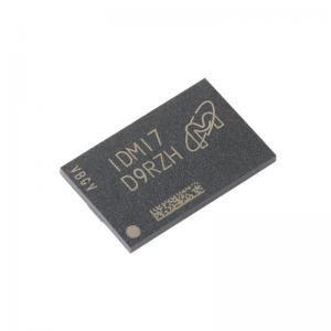
| FBGA Code | D9RZH |
| 16 bit | |
| 64 M x 16 | |
| 1 Gbit | |
| 400 MHz | |
| 1.9 V | |
| 1.7 V | |
| 95 mA | |
| 0 C | |
| + 85 C |
Description
The DDR2 SDRAM uses a double data rate architecture to achieve high-speed opera-tion. The double data rate architecture is essentially a 4n-prefetch architecture, with an interface designed to transfer two data words per clock cycle at the I/O balls. A single READ or WRITE operation for the DDR2 SDRAM effectively consists of a single 4n-bitwide, two-clock-cycle data transfer at the internal DRAM core and four corresponding n-bit-wide, one-half-clock-cycle data transfers at the I/O balls.
A bidirectional data strobe (DQS, DQS#) is transmitted externally, along with data, for use in data capture at the receiver. DQS is a strobe transmitted by the DDR2 SDRAM during READs and by the memory controller during WRITEs. DQS is edge-aligned with data for READs and center-aligned with data for WRITEs. The x16 offering has two data strobes, one for the lower byte (LDQS, LDQS#) and one for the upper byte (UDQS, UDQS#).
The DDR2 SDRAM operates from a differential clock (CK and CK#); the crossing of CK going HIGH and CK# going LOW will be referred to as the positive edge of CK. Com-mands (address and control signals) are registered at every positive edge of CK. Input data is registered on both edges of DQS, and output data is referenced to both edges of DQS as well as to both edges of CK.
Absolute Maximum DC Ratings
Notes: 1. VDD, VDDQ, and VDDL must be within 300mV of each other at all times; this is not required when power is ramping down.
2. VREF 0.6 × VDDQ; however, VREF may be ุ VDDQ provided that VREF 300mV.
3. Voltage on any I/O may not exceed voltage on VDDQ.
Features
• VDD = 1.8V ±0.1V, VDDQ = 1.8V ±0.1V
• JEDEC-standard 1.8V I/O (SSTL_18-compatible)
• Differential data strobe (DQS, DQS#) option
• 4n-bit prefetch architecture
• Duplicate output strobe (RDQS) option for x8
• DLL to align DQ and DQS transitions with CK
• 8 internal banks for concurrent operation
• Programmable CAS latency (CL)
• Posted CAS additive latency (AL)
• WRITE latency = READ latency - 1 t CK
• Selectable burst lengths (BL): 4 or 8
• Adjustable data-output drive strength
• 64ms, 8192-cycle refresh
• On-die termination (ODT)
• Industrial temperature (IT) option
• Automotive temperature (AT) option
• RoHS-compliant
• Supports JEDEC clock jitter specification
Trading Guides
| Shipping | Delivery period | For in-stock parts, orders are estimated to ship out in 3 days. |
| Shipping rates | After confirming the order, we will evaluate the shipping cost based on the weight of the goods | |
| Shipping option | We provide DHL, FedEx, EMS, SF Express, and Registered Air Mail international shipping. | |
| Shipping tracking | We will notify you by email with tracking number once order is shipped. | |
Returning warranty | Returning | Returns are normally accepted when completed within 30 days from date of shipment.Parts should be unused and in original packaging.Customer has to take charge for the shipping. |
| Warranty | All Retechip purchases come with a 30-day money-back return policy, This warranty shall not apply to any item where defects have been caused by improper customer assembly, failure by customer to follow instructions, product modification, negligent or improper operation | |
| Ordering | Payment | T/T,PayPal, Credit Card includes Visa, Master, American Express. |