
Add to Cart
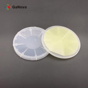
4H SiC Epitaxial Wafer 0.015Ω•cm—0.025Ω•cm ≤4000/cm2 150.0 mm +0mm/-0.2mm
JDCD03-001-003
Overview
The next type is beta silicon carbide. Beta SiC is produced at
temperatures higher than 1700 degrees Celsius. Alpha carbide is the
most common, and has a hexagonal crystal structure similar to
Wurtzite. The beta form is similar to diamond, and is used in a few
applications. It has been the preferred choice in power semis for
electric vehicles. Several third-party SiC wafer suppliers are
currently working on this new material.
Property | P-MOS Grade | P-SBD Grade | D Grade |
| Crystal Form | 4H | ||
| Polytype | None Permitted | Area≤5% | |
| (MPD) a | ≤0.2 /cm2 | ≤0.5 /cm2 | ≤5 /cm2 |
| Hex Plates | None Permitted | Area≤5% | |
| Hexagonal Polycrystal | None Permitted | ||
| Inclusions a | Area≤0.05% | Area≤0.05% | N/A |
| Resistivity | 0.015Ω•cm—0.025Ω•cm | 0.015Ω•cm—0.025Ω•cm | 0.014Ω•cm—0.028Ω•cm |
| (EPD)a | ≤4000/cm2 | ≤8000/cm2 | N/A |
| (TED)a | ≤3000/cm2 | ≤6000/cm2 | N/A |
| (BPD)a | ≤1000/cm2 | ≤2000/cm2 | N/A |
| (TSD)a | ≤600/cm2 | ≤1000/cm2 | N/A |
| Stacking Fault | ≤0.5% Area | ≤1% Area | N/A |
Surface Metal Contamination | (Al, Cr, Fe, Ni, Cu, Zn, Pb, Na, K, Ti, Ca ,V, Mn) ≤1E11 cm-2 | ||
| Diameter | 150.0 mm +0mm/-0.2mm | ||
| Surface Orientation | Off-Axis:4°toward <11-20>±0.5 ° | ||
| Primary Flat Length | 47.5 mm ± 1.5 mm | ||
| Secondary Flat Length | No Secondary Flat | ||
| Primary Flat Orientation | Parallel to<11-20>±1° | ||
| Secondary Flat Orientation | N/A | ||
| Orthogonal Misorientation | ±5.0° | ||
| Surface Finish | C-Face:Optical Polish,Si-Face:CMP | ||
| Wafer Edge | Beveling | ||
Surface Roughness (10μm×10μm) | Si Face Ra≤0.20 nm ; C Face Ra≤0.50 nm | ||
| Thickness a | 350.0μm± 25.0 μm | ||
| LTV(10mm×10mm)a | ≤2μm | ≤3μm | |
| (TTV)a | ≤6μm | ≤10μm | |
| (BOW) a | ≤15μm | ≤25μm | ≤40μm |
| (Warp) a | ≤25μm | ≤40μm | ≤60μm |
| Chips/Indents | None Permitted ≥0.5mm Width and Depth | Qty.2 ≤1.0 mm Width and Depth | |
Scratches a (Si Face,CS8520) | ≤5 and Cumulative Length≤0.5×Wafer Diameter | ≤5 and Cumulative Length≤1.5×Wafer Diameter | |
| TUA(2mm*2mm) | ≥98% | ≥95% | N/A |
| Cracks | None Permitted | ||
| Contamination | None Permitted | ||
| Property | P-MOS Grade | P-SBD Grade | D Grade |
| Edge Exclusion | 3mm | ||
Remark: 3mm edge exclusion is used for the items marked with a.
About Us
We specialize in processing a variety of materials into wafers, substrates and customized optical glass parts.components widely used in electronics, optics, opto electronics and many other fields. We also have been working closely with many domestic and oversea universities, research institutions and companies, provide customized products and services for their R&D projects. It's our vision to maintaining a good relationship of cooperation with our all customers by our good reputations.
FAQ
Q: Are you trading company or manufacturer ?
We are factory.
Q: How long is your delivery time?
Generally it is 3-5 days if the goods are in stock.
or it is 7-10 days if the goods are not in stock, it is according
to quantity.
Q: Do you provide samples ? is it free or extra ?
Yes, we could offer the sample for free charge but do not pay the
cost of freight.
Q: What is your terms of payment ?
Payment <=5000USD, 100% in advance.
Paymen >=5000USD, 80% T/T in advance , balance before shippment.

