
Add to Cart
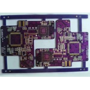
HDI PCB Board means as high-density interconnect PCB, is a kind of PCB with a higher wiring density per unit area than traditional boards.
HDI boards are more compact and have smaller vias, pads, copper traces and spaces.
As a result, HDIs have denser wiring resulting in lighter weight, more compact, lower layer count PCBs.
HDI PCB is more fit into the little spaces and have a smaller amount of mass than conservative PCB designs.
Advantages of HDI PCB: High Component Density; Space-saving; Lightweight Boards; Fast Processing; Save Number of Layers; Accommodate Low Pitch Packages; High Reliability
Factory Capabilities
| FACTORY CAPABILITIES | |||
| No. | Items | 2019 | 2020 |
| 1 | HDI Capabilities | HDI ELIC (4+2+4) | HDI ELIC(5+2+5) |
| 2 | Max layer count | 32L | 36L |
| 3 | Board Thickness | Core thickness 0.05mm-1.5mm ,Fineshed board thickness 0.3-3.5mm | Core thickness 0.05mm-1.5mm ,Fineshed board thickness 0.3-3.5mm |
| 4 | Min.Hole Size | Laser 0.075mm Mechnical 0.15 | Laser 0.05mm Mechnical 0.15 |
| 5 | Min Line Width/Space | 0.035mm/0.035 | 0.030mm/0.030mm |
| 6 | Copper Thickness | 1/3oz-4oz | 1/3oz-6oz |
| 7 | Size Max Panel size | 700x610mm | 700x610mm |
| 8 | Registration Accuracy | +/-0.05mm | +/-0.05mm |
| 9 | Routing Accuracy | +/-0.075mm | +/-0.05mm |
| 10 | Min.BGA PAD | 0.15mm | 0.125mm |
| 11 | Max Aspect Ratio | 10:1 | 10:1 |
| 12 | Bow and Twist | 0.50% | 0.50% |
| 13 | Impedance Control Tolerance | +/-8% | +/-5% |
| 14 | Daily output | 3,000m2 (Max capacity of equipment) | 4,000m2 (Max capacity of equipment) |
| 15 | Surface Finishing | HASL Lead Free /ENEPING /ENIG /HASL /FINGER GOLD/IMMERSION TIN/SELECTIVE THICK GOLD | |
| 16 | Raw Material | FR-4/Normal Tg/High Tg/Low Dk/HF FR4/PTEE/PI | |
| PCBA Capability | |||
| Material Type | Item | Min | Max |
| PCB | Dimension (length,width,height.mm) | 50*40*0.38 | 600*400*4.2 |
| Material | FR-4,CEM-1,CEM-3,Aluminium-based board,Rogers,ceramic plate,FPC | ||
| Surface finish | HASL,OSP,Immersion gold,Flash Gold Finger | ||
| Components | Chip&IC | 1005 | 55mm |
| BGA Pitch | 0.3mm | - | |
| QFP Pitch | 0.3mm | - | |
1.through vias from surface to surface,
2.with buried vias and through vias,
3.two or more HDI layer with through vias,
4.passive substrate with no electrical connection,
5.coreless construction using layer pairs
6.alternate constructions of coreless constructions using layer
pairs.
Board Cut - Inner Wet film -DES - AOI - Brown Oxido - Outer Layer Press - Out Layer Lamination - X-RAY & Rounting - Copper reduce & brown oxide - Laser Drilling - Drilling - Desmear PTH - Panel plating - Outer Layer dry film - Etching - AOI- Impedance Testing - S/M Pluged hole - Solder Mask - Component Mark - Impedance testing - Immersion Gold -V-cut - Routing - Electrical Test - FQC - FQA -Package -Shipment
Automotive and aerospace industries, where lower weight can mean more efficient operation, have been utilizing HDI PCBs at an increasing rate. such as onboard WiFi and GPS, rearview cameras and backup sensors rely on HDI PCBs. As automotive technology continues to advance, HDI tech will likely play an increasingly important role.
HDI PCBs are also prominently featured in medical devices; advanced electronic medical devices such as equipment for monitoring, imaging, surgical procedures, laboratory analysis etc., and incorporate HDI boards. The high-density technology promotes improved performance and smaller, more cost-effective devices, potentially improving the accuracy of monitoring and medical testing.
Industrial automation requires abundant computerization, and IoT devices are becoming more common in manufacturing, warehousing, and other industrial settings. Many of these advanced equipment employ HDI technology. Today, businesses use electronic tools to keep track of inventory and monitor equipment performance. Increasingly, machinery includes smart sensors that collect usage data and connect to the internet to communicate with other smart devices, as well as to relay information to management and help optimize operations.
Except mentioned above, you'll also can find high-density interconnect PCBs in all types of digital devices, like smartphones and tablets, in automobiles, aircraft , mobile /cellular phones, touch-screen devices, laptop computers, digital cameras, 4/5G network communications, and military applications such as avionics and smart munitions.
| Product Type | Qty | Normal lead time | Quick-turn lead time |
| SMT+DIP | 1-50 | 1WD-2WD | 8H |
| SMT+DIP | 51-200 | 2WD-3WD | 1.5WD |
| SMT+DIP | 201-2000 | 3WD-4WD | 2WD |
| SMT+DIP | ≥2001 | 4WD-5WD | 3WD |
| PCBA(2-4Layer) | 1-50 | 2.5WD-3.5WD | 1WD |
| PCBA(2-4Layer) | 51-2000 | 5WD-6WD | 2.5WD |
| PCBA(2-4Layer) | ≥2001 | ≥7WD | 5WD |
| PCBA(6-10Layer) | 1-50 | 3WD-4WD | 2.5WD |
| PCBA(6-10Layer) | 51-2000 | 7WD-8WD | 6WD |
| PCBA(10-HDILayer) | 1-50 | 7WD-9WD | 5WD |
| PCBA(10-HDILayer) | 51-2000 | 9WD-11WD | 7WD |
PCB: Vacuum packaging with carton box
PCBA: ESD packaging with carton box