
Add to Cart
HDI PCB Board, also known as high-density interconnect PCB, is a kind of PCB with a higher wiring density per unit area than traditional boards. HDI boards are more compact and have smaller vias, pads, copper traces and spaces. As a result, HDIs have denser wiring resulting in lighter weight, more compact, lower layer count PCBs. HDI PCB is more fit into the little spaces and have a smaller amount of mass than conservative PCB designs.
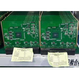
Haina Lean provide One-stop PCB Board Favrication and assembly service , include :SMT Assembly , BGA Assembly , HDI ,Through-Hole Assembly ,Mixed Assembly,Rigid Flex PCB Assembly services . etc.
| FACTORY CAPABILITIES | |||
| No. | Items | 2019 | 2020 |
| 1 | HDI Capabilities | HDI ELIC (4+2+4) | HDI ELIC(5+2+5) |
| 2 | Max layer count | 32L | 36L |
| 3 | Board Thickness | Core thickness 0.05mm-1.5mm ,Fineshed board thickness 0.3-3.5mm | Core thickness 0.05mm-1.5mm ,Fineshed board thickness 0.3-3.5mm |
| 4 | Min.Hole Size | Laser 0.075mm Mechnical 0.15 | Laser 0.05mm Mechnical 0.15 |
| 5 | Min Line Width/Space | 0.035mm/0.035 | 0.030mm/0.030mm |
| 6 | Copper Thickness | 1/3oz-4oz | 1/3oz-6oz |
| 7 | Size Max Panel size | 700x610mm | 700x610mm |
| 8 | Registration Accuracy | +/-0.05mm | +/-0.05mm |
| 9 | Routing Accuracy | +/-0.075mm | +/-0.05mm |
| 10 | Min.BGA PAD | 0.15mm | 0.125mm |
| 11 | Max Aspect Ratio | 10:1 | 10:1 |
| 12 | Bow and Twist | 0.50% | 0.50% |
| 13 | Impedance Control Tolerance | +/-8% | +/-5% |
| 14 | Daily output | 3,000m2 (Max capacity of equipment) | 4,000m2 (Max capacity of equipment) |
| 15 | Surface Finishing | HASL Lead Free /ENEPING /ENIG /HASL /FINGER GOLD/IMMERSION TIN/SELECTIVE THICK GOLD | |
| 16 | Raw Material | FR-4/Normal Tg/High Tg/Low Dk/HF FR4/PTEE/PI | |
| PCBA Capability | |||
| Material Type | Item | Min | Max |
| PCB | Dimension (length,width,height.mm) | 50*40*0.38 | 600*400*4.2 |
| Material | FR-4,CEM-1,CEM-3,Aluminium-based board,Rogers,ceramic plate,FPC | ||
| Surface finish | HASL,OSP,Immersion gold,Flash Gold Finger | ||
| Components | Chip&IC | 1005 | 55mm |
| BGA Pitch | 0.3mm | - | |
| QFP Pitch | 0.3mm | - | |
1.through vias from surface to surface,
2.with buried vias and through vias,
3.two or more HDI layer with through vias,
4.passive substrate with no electrical connection,
5.coreless construction using layer pairs
6.alternate constructions of coreless constructions using layer
pairs.
Board Cut - Inner Wet film -DES - AOI - Brown Oxido - Outer Layer Press - Out Layer Lamination - X-RAY & Rounting - Copper reduce & brown oxide - Laser Drilling - Drilling - Desmear PTH - Panel plating - Outer Layer dry film - Etching - AOI- Impedance Testing - S/M Pluged hole - Solder Mask - Component Mark - Impedance testing - Immersion Gold -V-cut - Routing - Electrical Test - FQC - FQA -Package -Shipment
| PCB design | Product Assembly |
SMT Assembly: PTH Assembly: PCB Fabrication: Component procurement: | Complete turnkey solutions Function Test & Inspection: |
1.High Component Density
2.Space-saving
3.Lightweight Boards
4.Fast Processing
5.Save Number of Layers
6.Accommodate Low Pitch Packages
7.High Reliability
Automotive and aerospace industries, where lower weight can mean more efficient operation, have been utilizing HDI PCBs at an increasing rate. such as onboard WiFi and GPS, rearview cameras and backup sensors rely on HDI PCBs. As automotive technology continues to advance, HDI tech will likely play an increasingly important role.
HDI PCBs are also prominently featured in medical devices; advanced electronic medical devices such as equipment for monitoring, imaging, surgical procedures, laboratory analysis etc., and incorporate HDI boards. The high-density technology promotes improved performance and smaller, more cost-effective devices, potentially improving the accuracy of monitoring and medical testing.
Industrial automation requires abundant computerization, and IoT devices are becoming more common in manufacturing, warehousing, and other industrial settings. Many of these advanced equipment employ HDI technology. Today, businesses use electronic tools to keep track of inventory and monitor equipment performance. Increasingly, machinery includes smart sensors that collect usage data and connect to the internet to communicate with other smart devices, as well as to relay information to management and help optimize operations.
Except mentioned above, you'll also can find high-density interconnect PCBs in all types of digital devices, like smartphones and tablets, in automobiles, aircraft , mobile /cellular phones, touch-screen devices, laptop computers, digital cameras, 4/5G network communications, and military applications such as avionics and smart munitions.
| Product Type | Qty | Normal lead time | Quick-turn lead time |
| SMT+DIP | 1-50 | 1WD-2WD | 8H |
| SMT+DIP | 51-200 | 2WD-3WD | 1.5WD |
| SMT+DIP | 201-2000 | 3WD-4WD | 2WD |
| SMT+DIP | ≥2001 | 4WD-5WD | 3WD |
| PCBA(2-4Layer) | 1-50 | 2.5WD-3.5WD | 1WD |
| PCBA(2-4Layer) | 51-2000 | 5WD-6WD | 2.5WD |
| PCBA(2-4Layer) | ≥2001 | ≥7WD | 5WD |
| PCBA(6-10Layer) | 1-50 | 3WD-4WD | 2.5WD |
| PCBA(6-10Layer) | 51-2000 | 7WD-8WD | 6WD |
| PCBA(10-HDILayer) | 1-50 | 7WD-9WD | 5WD |
| PCBA(10-HDILayer) | 51-2000 | 9WD-11WD | 7WD |
PCB: Vacuum packaging with carton box
PCBA: ESD packaging with carton box
Q1:What kind of PCB file format can you accept for production?
Gerber, PROTEL 99SE, PROTEL DXP, CAM350, ODB+(.TGZ)
Q2:Is my PCB files safe when I submit them to you for manufacturing?
We respect customer's copyright and will never manufacture PCB for someone else with your files unless we receive written permission from you, nor we'll share these files with any other 3rd parties.
Q3:What payments do you accept ?
-Telex Transfer(T/T),Western Union,Letter of Credit(L/C)
-Paypal,AliPay,Credit Card
Q4:How to get the PCB?
A:For small packages, we will ship the boards to you by
DHL,UPS,FedEx,EMS. Door to door service! You will get your PCBs at
your home.
B:For heavy goods more than 300kg, we may ship your boards by ship
or by air to save freight cost. Of course, if you have your own
forwarder, we may contact them for dealing with your shipment.
Q5:What is your minimum order quantity?
Our MOQ is 1 PCS.
Q6: Can we visit your company?
No problem. You are welcome to visit us in Beijing. Or the branch factory is in Tianjin.
Q7: How can you ensure the quality of the PCB?
Our PCBs are 100% test including Flying Probe Test, E-test and AOI.
Beijing Haina lean Electronics Co.,Ltd is one of the most professional PCB manufacture in Beijing,China. With more then 10 years of development, Haina Lean Electronics turns into a first class manufacture of HDI PCB ,with production capability 4000 square meters.
Our factory is providing high quality bare PCB, PCB layout design service and PCB assembly service,including components sourcing, function test,conformal coating and complete assembly for clients all.
We have profuse experience in manufacturing PCB,owned experienced technical R & D technology team, young and professional sales and customer service team, experienced and professional procurement team and assembly testing team, which make sure the products quality of the pass rate, on-time delivery rate of customer orders.
Our services include: circuit board design and layout, 2-46 layers PCB manufacturing, professional FPC production, electronic components purchasing, SMT professional processing, Soldering and Assembly, especially sample and small bulk orders. we have the advantages of a quick quote, fast production, fast delivery.
The company pursues "inclusiveness, excellence, people-oriented". Constantly innovate, take technology as the core, regard quality as life, and wholeheartedly provide customers with high-quality and high-efficiency humanized services.We are willing to serve our customers with the principle of continuous honesty & trustworthiness, pragmatism and innovation.