Add to Cart
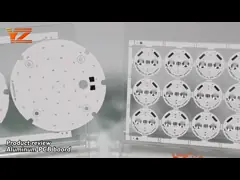
LED Pcb Board Aluminum Base 1.0mm 1.2m 1.5m Circuit Board Mcpcb
• Thick Copper Foil Etching
Aluminum PCBs are usually applied in power devices with high power
density so copper foil is relatively thick. When copper foil is 3oz
thick or more, copper foil etching requires trace width
compensation. Otherwise, trace width will be out of tolerance after
etching. Therefore, to guarantee optimal trace width/spacing and
impedance control that are able to meet design demands, the
following work has to be finished in advance.
a. Trace width compensation should be appropriately designed.
b. The effect of trace manufacturing on trace width/spacing should
be eliminated.
c. Etching factors and agent parameters should be rigorously
controlled.
• Solder Mask Printing
Solder mask printing is regarded as a manufacturing difficulty of
aluminum PCB fabrication due to effect of thick copper foil. If
trace copper thickness is extraordinary after image etching, a
large difference will be generated between trace surface and base
board and solder mask will become difficult. To ensure smooth
solder mask printing, the following principles should be conformed
to:
a. Solder mask oil should be picked up with high-quality
performance.
b. Two-time solder mask printing is used.
c. When necessary, the manufacturing method of resin filling first
and solder mask second is relied on.
• Mechanical Manufacturing
Mechanical manufacturing of aluminum PCBs contain mechanical
drilling, milling and molding and v-scoring and burr tends to be
left on internal via, which will reduce electric strength.
Therefore, to ensure high-quality mechanical manufacturing, the
following principles should be stuck to:
a. Electric milling and professional milling cutter should be
picked up for low-volume production.
b. Control technique and pattern should be noticed in the process
of die molding.
c. Drilling parameters should be appropriately adjusted on
thick-copper aluminum PCBs to prevent burr from generating.
| Item | Capacity |
| Base material | Aluminum |
| Layers | 1-2 |
| Finished inner/Outer copper thickness | 1-6OZ |
| Finished board thickness | 0.2-7.0mm |
| Min hole size | mechanical size: 0.15mm Laser size:0.1mm |
| Impedance | +/-5% |
| Plugging vias capability | 0.2-0.8mm |
| Outline profile | Rout/V-cut/Bridge/stamp hole |
| surface treatmentreatmentSi | HASL,HASL lead free,immersion gold,immersion Tin,immersion silver,hard gold,flash gold,OSP,etc |
FAQ:
Q1. What specifications do you need for PCB quotation?
A: We need your PCB Gerber file,board thickness,copper
thickness,surface finishing and quantity to quote you.
Q2. How can I get a sample to check your quality?
A: After price confirmation,you can place orders for samples for your
testing and evaluation.
Q3: How long can I receive the sample?
A: After you make a payment and send us confirmed files,your samples will be ready within 3-5 work days.