
Add to Cart
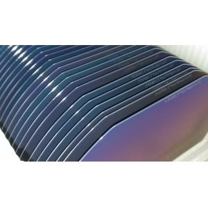
Silicon Wafer for integrated circuits , detector / sensor device , MEMS fabrication and solar cells
We are a supplier of CZ and FZ silicon wafer and has been the worldwide source for high pure silicon wafers & thermal oxide silicon materials . Silicon wafer is the most common material and widely used for a varity of high-tech industries , including integrated circuits , detector / sensor device , MEMS fabrication, opto-electronic components, and solar cells . With abundant selling and production experiences , we understand your requirements and can provide exactly the silicon products you need with the highest quality and lowest possible price . We can provide both standard and customized silicon wafers to meet your unique needs . Silicon wafer is produced as per SEMI. Standard and packed in standard cassette with vacuum sealed in clean room enviroment , with a good quality control system , we are dedicated to providing clean and high quality silicon wafer products . For standard and frequently used silicon wafer , we always maintains a large inventory including prime wafers and test wafers to insure we can satisfy your requirements in a timely manner . As for non-standard silicon wafer , this is our strength , we have the ability to help customers in finding hard to find or odd silicon wafer . We specialized in providing not only bare silicon wafer but also in providing value added silicon products , we can grow thermal oxide ( SiO2 layer ) and deposit silicon nitride ( Si3N4 layer ) onto bare silicon substrate in diameter range from 2 inch to 12 inch , we are ready to work with you for your specific silicon needs . Please contact us for further silicon wafer information .
Silicon Wafer Available
CZ or FZ Wafer | Prime Wafer |
Intrinsic Wafer | Test Wafer |
Heavily Doped Wafer | High Resistivity Wafer |
Off Axis Orientation Wafer | Special Orientation Wafer |
Ultra Flat Wafer | Ultra Thin Wafer |
Ultra Thick Wafer | Double Sides Polished |
Thermal Oxide Wafer | Epi Wafer |
Product Specification
Growth | CZ / FZ |
|---|---|
Diameter | Ø 2" / Ø 3" / Ø 4" / Ø 6" / Ø 8" / Ø 12" |
Thickness | 275 um ~ 775 um |
Orientation | <100> / <111> / <110> or others |
Conductivity | P - type / N - type / intrinsic |
Dopant | Boron / Phosphorous / Antimony / Arsenic |
Resistivity | 0.001 ~ 10000 ohm-cm |
Surface | One side polished / two sides polished |
TTV | <= 10 um |
Bow / Warp | <= 40 um |
Grade | Prime / Test / Dummy grade |