
Add to Cart
ZnO Wafer, CdS wafer, CdSe wafer, CdTe wafer, ZnS wafer, ZnSe wafer and ZnTe wafer
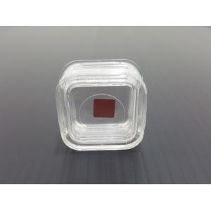
We provides high purity single crystal ZnO wafer and ZnO bulk for power device , LED , sensor and detector applications . With an ideal crystal structure , ZnO wafer ( Zinc oxide ) has a 2% lattice mismatch to GaN , that is much less than the lattice mismatch of sapphire wafer and SiC wafer . ZnO wafer is one of the most suitable substrate for using as GaN epitaxial growth and wide band gap semiconductor application . ZnO wafer are supplied in square shape , undoped , size 10 x 10 x 0.5 mm , double sides polished surface finish and oriented , our high quality ZnO wafer have been widely used for the growth of
nitride base devices . Please contact us for more product information .
ZnO Wafer Application
| GaN epitaxial growth | UV detectors |
| Power devices | Light-emitting devices |
| Photovoltaic | Sensors |
ZnO Wafer Properties
| Chemical formula | ZnO |
| Crystal structure | Hexagonal |
| Lattice constant | 3.3 A |
| Lattice mismatch with GaN in <0001> plane | 9 |
| Thermal conductivity | 0.006 cal / cm /K |
| Refractive index | 2.0681 / 2.0510 |
| Identified polished face | Zn - face / O - face |
Product Specification
| Growth | Hydrothermal |
|---|---|
| ZnO bulk / block | 26.5 x 26.5 x 10 mm |
| ZnO wafer | 10 x 10 x 0.5 mm |
| Orientation | Zn face <0001> / O face <000-1> |
| Resistivity | 500 - 1000 ohm-cm |
| Surface | two sides polished |
| Roughness | Ra <= 10 A |
| Package | Membrance box |

