
Add to Cart
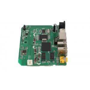
PCBA Prototype Power Communication Pcba Component Sourcing Fast PCBA
Shenzhen Yideyi Technology Co., Ltd provide full turnkey contract
included Custom design, PCB prototype, PCB, PCBA, PCB Assembly,
testing, accessories and cables, plastic enclosure,and
packaging.box building.
EMS include consumers electronic ,medicla, industrial,power
control, automotive. Temperature & Humidity ,Internet &
Communication Smart Home Security etc device .
OEM PCB and PCBA Manufacturer
1. 5 hours for pcba prototype, no MOQ (MOQ can be 1pcs,30 models PCB prototype per day, 3 million points per day.
2. Mature ISO9001 quality management system,IATF16949:2016
international automotive quality system standard and ISO13485:2016
medical device quality management system.
3. High-precision production machine, 5000 square meters dust-free
anti-static workshop, strict workshop temperature and humidity
monitoring.
4. 10 years of pcb & pcba manufacturing production and export
experience, Famous brand manufacturers in China.
5. ERP order management system, one-click extraction of historical
data , component inventory management is more convenient.
6. Free 24 hour online service among worldwide, problems feedback
are no longer delayed.
7. Professional engineering team with an average of 10 years of
industry experience.
8. NDA. We are willing to sign NDA effect by customer side local
law and promising to keep customers data in high confidential
level.
PCBA Capability
| Board Type | Rigid, Flexible, Rigid-flexible |
| Base Material | FR4, High TG FR4, CEM1,CEM3,Aluminum, Rogers, Taconic |
| Layer Counts | 1-30L |
| Max Board Size | 1200*400mm |
| Min Hole Size (mechanical) | 0.15mm |
| Min Hole Size (laser) | 0.10mm |
| Controlled Tolerance | +/-5% |
| Copper Weight | 0.5-4oz |
| Outline Profile | Rout/ V-cut/ Bridge/ Stamp hole |
| Solder Mask | Double-sided green LPI,Also support Red,White,Yellow,Blue,Black |
| Silk Screen | Double-sided or single-sided in white,yellow,black,or negative |
| Surface Finish | HASL, HASL lead free, Immersion Gold, Immersion Tin, Immersion Silver, Hard gold, Flash gold, OSP |
Our Services & advantage:
YDY is the best pcb manufacturing and pcb assembly factory
globally, with ISO9001, ISO13485, 14000, and IATF16949 certificates
simultaneously.
We keeps pace with the times, has imported advanced YAMAHA, MADATA, selective wave soldering, 3D AOI, X-RAY etc equiments, we can provide original package componets agent service, custom pcb manufacturing, precise pcb assembly, accurate pcb printing, save your cost and time at the same time.
All PCBA are double Check by Machines and QC work.
PCBA application:aerospace pcba, military pcba, communication pcba, industrial pcba, medical pcba, automotive pcba etc.
FAQ:
Q1. How to you make the impedance calculation?
The impedance control system is done using some test coupons, the
SI6000 soft and the CITS 500s equipment from POLAR INSTRUMENTS.
The equipment measures the impedance on a representative track
configuration coupon of which the client has given us a determinate
value and tolerance.
Q2. What kind of PCB file format can you accept for production?
Gerber, PROTEL 99SE, PROTEL DXP, CAM350, ODB+(.TGZ)
Q3. How do we ensure quality?
Our high quality standard is achieved with the following.
1. The process is strictly controlled under ISO 9001:2008
standards.
2. Extensive use of software in managing the production process
3. State-of-art testing equipments and tools. E.g. Flying Probe,
X-ray Inspection, AOI (Automated Optical Inspector) and ICT
(in-circuit testing).
4. Dedicated quality assurance team with failure case analysis
process
5. Continuous staff training and education
Q4. How can we guarantee you receive an good quality product?
For PCB, we will use Flying Probe Test, E-test etc. for it.
For PCBA, we need you to offer us a method or test fixture for the
function test.Before that, our inspectors will use microscope and
X-ray to check the IC footwelding or bad solder etc.
Q5. What’s the key equipments for HDI manufacturing?
Key equipment list is as following: Laser drilling machine,
Pressing machine, VCP line, Automatic Exposing machine, LDI and
etc.
Q6. What’s the typical process flow for multi-layer PCB?
Material cutting → Inner dry film → inner etching → Inner AOI →
Multi-bond→ Layer stack up Pressing → Drilling → PTH → Panel
Plating → Outer Dry Film → Pattern Plating → Outer etching → Outer
AOI → Solder Mask → Component Mark → Surface finish → Routing → E/T
→ Visual Inspection.


