
Add to Cart
RoHS Soldering Using Tin-Lead Solder PTH Plated Through Hole PCB
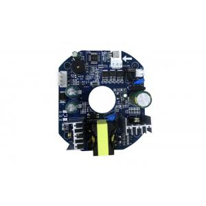
Assembly
We are fully equipped to handle the following through-hole PCB assembly services:
Manual and automated placement of components
Double Wave Flow Solder
RoHS soldering using tin-lead solder
Functional testing
Through-Hole PCB Assembly comes with a range of benefits including:
Withstanding stress
Perfect for large components
High heat tolerance
Ease of Prototyping
High Reliability
PCB Manufacture Capacity
| Service | RoHS Soldering Using Tin-Lead Solder PTH Plated Through Hole PCB Assembly |
| Base Material | FR-4 / High TG FR-4 / Halogen Free material |
| Number of Layers | 1-22Layers |
| Surface Finish | HASL(LF), Gold plating, Electroless nickel immersion gold, Immersion Tin, OSP(Entek) |
| Finish Board Thickness | 0.2mm-6.00 mm(8mil-126mil) |
| Finised inner/outer copper thickness | 1/2 oz min;12 oz max |
| Solder Mask | Green/Black/White/Red/Blue/Yellow |
| Min.Trace Width & Line Spacing | 0.075mm/0.1mm(3mil/4mil) |
| Min.Hole Diameter for CNC Driling | 0.1mm(4mil) |
| Min.Hole Diameter for punching | 0.9mm(35mil) |
| Biggest panel size | 610mm*508mm |
| Hole Positon | +/-0.075mm(3mil) CNC Driling |
| Conductor Width(W) | 0.05mm(2mil)or; +/-20% of original artwork |
| Hole Diameter(H) | PTH L:+/-0.075mm(3mil); Non-PTH L:+/-0.05mm(2mil) |
| Outline Tolerance | 0.125mm(5mil) CNC Routing; +/-0.15mm(6mil) by Punching |
| Insulation Resistance | 10Kohm-20Mohm |
| Conductivity | <50ohm |
| Test Voltage | 10-300V |
| Panel Size | 110×100mm(min);660×600mm(max) |
| Layer-layer misregistration | 4 layers:0.15mm(6mil)max; 6 layers:0.25mm(10mil)max |
| Min.spacing between hole edge to circuity pqttern of an inner layer | 0.25mm(10mil) |
| Min.spacing between board oulineto circuitry pattern of an inner layer | 0.25mm(10mil) |
Our responsive sales and technical support team as well as our
prompt after sales services will make sure that you are taken care
of the entire way. Feel free to reach out to us with your bespoke
requirements and rest assured that you will be offered nothing but
the best. All you need to do is to share the following details with
us:
BOM Information.
Gerber Files that identify the areas of the board that should
receive solder.
In addition to PCB Assembly, be it through hole or surface mount,
at YDYPCBA we also undertake PCB assembly rework offering complete
reliability, high quality and optimal costs. Not only are we
well-versed in inventory management, fabrication and process
control, we also have a stringent control on vendor component
management.
FAQs:
1,Do you offer quick turn PCB Assembly ?
Yes, we offer 24 hours quick turn PCB Assembled Solution without
sacrifice the quality of the PCB Board.
2,Do you offer X-Ray capability ?
Yes, we inspect the boards using X-ray and therefore offer total
reliability.
3, Do you offer conformal coating service ?
Yes, conformal coating is a part of our value-added services.
4, Do you offer testing service ?
Yes, we offer robust functional testing that adds to the product
reliability.
5, Do you offer IPC 610 or J-STD Quality inspections ?
Absolutely, we offer these inspections as per client requirements.
6,Do you offer first article inspection ?
Yes, basis client requirements, we are well equipped to offer first
article inspection.
7, What is your standard turnatound time for PCB Assembly ?
Our standard turnaround time for PCB Assembly is 3 weeks.
8,What is the PCB Assembly cost ?
The cost is based on a number of factors including the types of PCB
parts, order quantity and more. Once you reach out to us with your
bespoke requirements, we will revert with a custom quote


