
Add to Cart
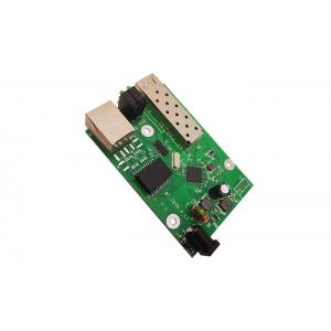
Quick Turn Prototype PCB Fabrication SMD DIP Through Hole Pcb Assembly.
YDY PCBA are fully equipped to handle the following through-hole PCB assembly services:
We have automated insertion equipment for placing components
axially or radially. We use various such equipment for high-speed
installation of through-hole components.
Reflow oven in our facility allows us to fix soldering paste
appropriately.
Automated wave soldering system allows us to precisely solder
through-hole components.
Advanced aqueous washing system for removing contaminants from the
circuit boards.
We use computer-controlled selective soldering machines for
reducing errors that may occur during tin-lead or RoHS Through-hole
assembly. This helps us reduce errors, as well as the costs of
manufacturing.
We provide in-house conformal coating, as well as device
programming.
All PCBs are built to ANSI/J-STD-001 and IPC-A-610-D standards.
PCB Manufacture Capacity
| Service type |
|
| Board materials | FR-4; high Tg; high CTI; halogen free; high frequency(rogers,taconic, PTFE,nelcon, ISOLA,polyclad 370 HR); thick copper |
| Surface Finish | HAL(with Pb free),plated Ni/Au, Immersion silver,Imm Ni/Au,Imm Sn, hard gold,OSP,ect |
| Finish Board Thickness | 0.2mm-6.00 mm(8mil-126mil) |
| Finished copper thickness | Outer layers: Min.thickness 1 OZ, Max.thickness 10 OZ Inner layers: Min.thickness 0.5OZ, Max.thickness 6 OZ |
| Solder Mask | Green/Black/White/Red/Blue/Yellow |
| Min.Trace Width & Line Spacing | 0.075mm/0.1mm(3mil/4mil) |
| Min.Hole Diameter for CNC Driling | 0.1mm(4mil) |
| Min.Hole Diameter for punching | 0.9mm(35mil) |
| Biggest panel size | 610mm*508mm |
| Hole Positon | +/-0.075mm(3mil) CNC Driling |
| Conductor Width(W) | 0.05mm(2mil)or; +/-20% of original artwork |
| Hole Diameter(H) | PTH L:+/-0.075mm(3mil); Non-PTH L:+/-0.05mm(2mil) |
| Outline Tolerance | 0.125mm(5mil) CNC Routing; +/-0.15mm(6mil) by Punching |
| Insulation Resistance | 10Kohm-20Mohm |
| Conductivity | <50ohm |
| Test Voltage | 10-300V |
| Panel Size | 110×100mm(min);660×600mm(max) |
| Layer-layer misregistration | 4 layers:0.15mm(6mil)max; 6 layers:0.25mm(10mil)max |
| Min.spacing between hole edge to circuity pqttern of an inner layer | 0.25mm(10mil) |
| Min.spacing between board oulineto circuitry pattern of an inner layer | 0.25mm(10mil) |
| Board thickness tolerance | 4 layers:+/-0.13mm(5mil); 6 layers:+/-0.15mm(6mil) |
| Impedance Control | +/-10% |
COMPANY PROFILE
1)In 2019, YDY Technology marked our 20th anniversary of providing
high quality PCB and PCBA service to the electronics industry. The
company is strong and professional technical, with perfect quality
assurance system and advances test-analyzed instrument. YDY is one
of the Professional PCB manufacturer from Shenzhen of China, We
have professional PCB designer for your PCB layout requirement. We
design single, double, and multi layers , Rigid, flexible,
Flex-Rigid printed circuit boards, and PCB assembly.
2) We have the ISO9001 & TS16949 certified.
3) 85% of our sales are oversea sales and export to Europe,United
sates and Asian.
4) Most of our boards are used for EMS, industrial, power, medical
and other products.
We YDY always take it as our mission by"Priority Customer, Effective Service", we insist in this management principle of "Development promote Management, Management benefit Efficiency". All of our employee keep firmly in mind with"High Quality ask for survival, High echnology ask for development ". We will strive to achieve our strategic objective:Professional Management, Large-scale Industry,International Market".


