In 2019, YDY Technology marked our 20th anniversary of providing high quality PCB and PCBA
service to the electronics industry. YDY has professional team to
offer flexible one stop solution for your PCBA projects, including
PCB design, components procurement, PCB Assembly, Box building,
functional test.Over the course of our 20+ years in business we
have successfully produced millions of pcbs and processed hundreds
of thousands of orders.
The electronic manufacture service is truly a detail intensive
business that requires a huge commitment to quality, service and
delivery. YDY provide PCB and PCBA with high-precision and have
earned our company an excellent reputation for consistent quality,
on-time delivery, and exceptional service.We are proud of the fact
that we have created true lasting partnerships with our customers.
It is a core value of our company and a key ingredient of what
makes us successful in what we do.Choosing YDY Technology, you will
save much time in your work and project!

YDY is a first-class manufacturer that could provide a full service
Electronic Manufacturing Services (EMS) provider.
We offer complete end to end manufacturing solutions,full turnkey
contract included custom design, PCB prototype, PCB, PCBA ,
high-level PCB Assembly, system level testing, accessories and
cables, plastic enclosure,packaging.box building and ect.
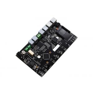
We manufactured include: from simple single sided PCB, double-sided
PCB to complex multilayer PCB up to 30 layers, Metal core PCB,
Flexible PCB, Rigid-flex PCB, HDI PCB, Microwave RF PCB and so on,
the pcb assembly service we offer based on our assembly plant
include: SMT, thru-hole, combo of SMT and thru-hole, consigned pcb
assembly, partial consigned pcb assembly and full turnkey pcb
assembly.
YDY specializes in high-quality, low-to-medium volume builds for
clients all over the world including North and South America,
Europe, Australia and Asia.
The key markets the company serve include security, power supply
& control, telecommunication, industrial control, automotive
electronics, medical and healthcare.
We have many experiences to developed smart watches,single
screen/dual screen cash register, smart face-sweeping cash
register, dual-screen integrated cash register, receipt printer,
barcode scanner, payment scanning box, smart cash box, self-service
electric stove control system, smart oxygen generator, smart watch
and ect according to customers' ideas and requirements:
Our engineering, quality assurance, and project management teams
cooperate closely with customers to fully understand and exceed
your requirements.
Our operations have been accredited ISO 9001:2015, ISO 13485:2016,
ISO 14001:2015 , IATF 16949:2016, and IPC-A-610 Class II and III.
Production capacity:
There are currently 6 SMT production lines, equipped with new
imported Siemens TX21, X2 mounter machines, automatic solder paste
printers, ten temperature zone reflow ovens, AOI, SPI and other
high-end equipment. The SMT production capacity is 25 million
solder joints/day, and is especially good at high-precision and
high-complexity single boards.
| SMT production | 25 million solder joints/day |
| SMT line | 6 |
Throwing rate | RC rate 0.3% |
| IC type no throwaway |
Single board type | POP/common board/FPC/rigid-flex board/metal substrate |
| Mounting component specifications | The smallest package | 01005 Chip/0.2 Pitch BGA |
| Minimum device accuracy | ±0.02mm |
| IC type patch accuracy | ±0.015mm |
| Mount PCB specifications | PCB size | 50*50mm-774*710mm |
| PCB thickness | 0.3-6.5mm |
Advantages of the development process:
YDY implements an advanced IPD integrated development process
system to ensure product development quality, and the new product
development cycle is shortened by more than 30% compared with the
industry average
◼ The time to put the product on the market is shortened by
40%~60%;
◼ Reduce product development time by 50% to 80%;
◼ Product development productivity increased by 25% to 30%;
◼ New product revenue (100% of total revenue) increased by 100%
DQE Implementation process:
Our goal is to provide high quality manufacturing services at a
competitive price.
Our service philosophy:
YDY Customer Support is committed to always providing the help you
need in a prompt and personalized manner – every day of the year –
no exceptions. Choosing YDY means you’re choosing the easiest
PCB/PCBA company to do business with.
Our Customer Support team sets the industry standard, and is backed
by over 20 years of experience in finding the PCB solution that
best fits your requirements. As a leading printed circuit board
solutions provider and manufacturer, we strive to partner with you
to ensure the success of your ideas and prototypes. Our product and
service innovations make us different than any other PCB company or
PCB manufacturer.
"YDY will support your design efforts like a member of your team.
We measure our success by your success!"