
Add to Cart
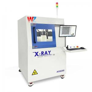
SMT 99.9% accuracy SMT PCB X-Ray Inspection Equipment X Ray Machine for LED TV Product Line
PCB X-Ray Inspection is a machine used for non-destructive testing and inspection of Printed Circuit Boards (PCBs). It utilizes X-rays to penetrate the electronic components and solder joints on the PCB, providing a detailed view of the internal structure and identifying any defects or faults.
The working principle of PCB X-Ray Inspection involves the following steps:
1. Preparation: The PCB is placed on a movable platform or conveyor belt within the inspection chamber. Any protective covers or components that may obstruct the X-ray penetration are removed.
2. X-ray Source: The machine consists of an X-ray tube that emits a controlled amount of X-rays. The X-ray energy level can be adjusted based on the density and thickness of the PCB materials.
3. X-ray Scanning: The X-ray source is directed towards the PCB, and the X-rays pass through the components and solder joints. The X-rays that penetrate the PCB are captured by a digital detector system.
4. Image Formation: The captured X-ray signals are processed by the machine's software algorithm to create a detailed image of the PCB's internal structure. The software enhances the contrast, sharpness, and resolution of the X-ray image for better analysis.
5. Defect Detection: The X-ray image is analyzed by the software to detect any defects or faults. These can include soldering issues, presence of voids or cracks in the solder joints, misalignment of components, electrical short circuits, or open circuits.
6. Inspection Analysis: The inspection results are displayed on a monitor for the operator or technician to evaluate. The software may provide measurement tools for accurate analysis of component dimensions, distances, and angles.
PCB X-Ray Inspection has a wide range of applications across various industries, including:
1. Electronics Manufacturing: It is used during the quality control process to inspect the integrity of the solder joints, ensuring proper connection and alignment of electronic components on the PCB.
2. Failure Analysis: In case of product failures or malfunctions, X-ray inspection helps identify the root cause by examining the internal structures and detecting any manufacturing defects, such as voids, cracks, or delamination.
3. Counterfeit Detection: X-ray inspection can reveal counterfeit electronic components by comparing their internal structures with genuine components, thereby preventing the use of counterfeit parts in electronic devices.
4. Research and Development: PCB X-Ray Inspection is also used in research and development laboratories to analyze new materials, evaluate new soldering techniques, and optimize PCB designs for better performance and reliability.
Introduction
X-Ray uses a cathode ray tube to generate high-energy electrons to
collide with a metal target. During the collision process, due to
the sudden deceleration of the electrons, the lost kinetic energy
will be released in the form of X-Ray. For the position of the
sample that cannot be detected by appearance, the change of light
intensity after X-Ray penetrates materials of different densities
is used to record the change of light intensity. Observe the
problematic area inside the analyte while destroying the analyte.
What is the principle of X-RAY equipment detection?
The detection principle of X-RAY equipment is basically X-ray
projection microscope. Under the action of high voltage, the X-ray
emission tube generates X-rays through the test sample (such as PCB
board, SMT, etc.), and then according to the density and atomic
weight of the sample material itself, and the X-rays will also have
different absorption. amount to produce an image on the image
receiver. The density of the measured workpiece determines the
intensity of the X-ray, and the higher the density, the darker the
shadow. The closer the X-ray tube is, the larger the shadow, and
vice versa, the smaller the shadow, which is the principle of
geometric magnification. Of course, not only the density of the
workpiece has an influence on the intensity of X-rays, but also the
intensity of X-rays can be adjusted through the voltage and current
of the power supply on the console. The operator can freely adjust
the imaging situation according to the imaging situation, such as
the display size of the image, the brightness and contrast of the
image, etc., and can also freely adjust and detect the part of the
workpiece through the automatic navigation function.
In conclusion, PCB X-Ray Inspection uses a combination of X-ray technology, imaging software, and analysis tools to provide a non-destructive inspection of PCBs. It helps ensure the quality, reliability, and performance of electronic products, and is an essential tool in the electronics manufacturing industry.
Features:
The device is cost-effective and supports flexible selection of
enhancers and high-definition FPD
The system has 600X magnification for high-definition real-time
imaging
User-friendly interface, various functions, and support for
graphical results
Support optional CNC high-speed movement automatic measurement
function
The standard configuration
●4/2 (optional 6-inch) image intensifier and megapixel digital
camera;
●90KV/100KV-5 micron X-ray source;
●Simple mouse click operation to write detection program;
●High detection repeatability;
Rotation and tilt of plus or minus 60 degrees, allowing a unique
viewing angle to detect samples;
●High-performance stage control;
●Large navigation window - easy to locate and identify defective
products;
●Automatic BGA detection program detects the bubbles of each BGA,
makes judgments according to customer requirements and outputs
Excel reports.
Purpose:
Defect detection of internal cracks and foreign objects in metal
materials and parts, plastic materials and parts, electronic
components, electronic components, LED components, etc., analysis
of internal displacement of BGA, circuit boards, etc.; Defects,
microelectronic systems and sealing components, cables, fixtures,
internal analysis of plastic parts.
Application range:
IC, BGA, PCB/PCBA, surface mount process solderability testing,
etc.